Introduction
Thermal relief plays a crucial role in PCB design, especially when working with copper zones for power and ground planes. For electronic hobbyists using KiCad, understanding KiCad thermal relief helps ensure reliable soldering while maintaining good electrical and thermal performance. Without proper thermal relief, large copper areas can act as heat sinks, making it hard to solder components by hand or even during reflow processes. This article explores what thermal relief is, why it matters, and step-by-step best practices on how to make thermal relief in KiCad. We will cover KiCad thermal pads, KiCad thermal vias, and tips for optimal heat dissipation. By following these guidelines, hobbyists can create robust boards that balance manufacturability and functionality.
What Is Thermal Relief and Why It Matters
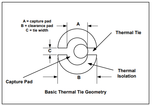
Thermal relief refers to the spoke-like copper connections between a component pad and a surrounding copper zone, such as a ground or power plane. These spokes provide electrical continuity while intentionally limiting thermal conductivity during soldering. In solid connections, the entire pad floods with copper, which rapidly draws heat away from the joint, leading to cold solder joints or incomplete wetting. Thermal relief spokes solve this by creating a higher thermal resistance path, allowing heat to stay localized at the pad.
This feature is particularly important for hobbyists prototyping boards with dense copper pours. Poor thermal management can cause soldering frustration, especially with through-hole or larger surface-mount parts. Industry standards like IPC-2221 emphasize thermal relief for pads connected to large conductor planes to improve solder joint quality. Effective KiCad thermal relief ensures your boards are easier to assemble at home, reduces rework, and supports better long-term reliability under heat stress. Ultimately, it bridges the gap between design intent and practical fabrication.
Technical Principles of Thermal Relief
The core principle behind thermal relief is balancing electrical, thermal, and mechanical properties in PCB connections. When a pad connects to a zone, KiCad generates spokes typically at 90-degree or 45-degree angles, depending on geometry. The spoke width and gap determine the connection's resistance: narrower spokes or larger gaps increase thermal isolation. This setup complies with soldering requirements outlined in standards such as J-STD-001, which address acceptable joint formation.
Heat dissipation occurs through the spokes and the zone itself, spreading warmth across the board. For high-power components, combining thermal relief with vias enhances this further. KiCad thermal vias act as vertical heat pipes, transferring heat from top-layer pads to inner or bottom layers. Thermal pads, often large exposed areas under ICs like QFNs, rely on these vias to avoid hotspots. The design must consider pad size, zone fill, and spoke count to prevent DRC violations like incomplete connections.
Copper zones in KiCad use algorithmic filling to respect clearances and connections. Parameters like minimum width ensure no fragile necks form during refill. Proper spoke count, usually at least two or three, guarantees redundancy if one fails during manufacturing. Hobbyists benefit from understanding these mechanics to avoid common pitfalls, such as spokes merging due to tight clearances.
How to Implement Thermal Relief in KiCad: Step-by-Step Guide
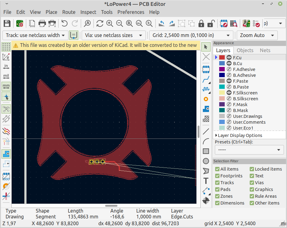
Implementing KiCad thermal relief starts with creating copper zones. Select the Add Filled Zone tool, draw the outline around your power or ground areas, and assign the net in Zone Properties. Under Pad Connection, choose "Thermal reliefs" for standard use or "Reliefs for PTH" if mixing pad types. Set Thermal Relief Gap to control spoke length and Spoke Width for thickness, leaving fields blank to inherit global values. Refill the zone with B hotkey to visualize the spokes.
For individual pads, right-click the pad, select Properties, and go to the Connections tab. Override zone settings here if needed, such as for high-current pins requiring solid fills. Board Setup under Constraints lets you define Minimum Thermal Relief Spoke Count to enforce rules via DRC. Run DRC after filling zones to catch issues like starved thermal reliefs, then add manual tracks if geometry blocks auto-spokes.
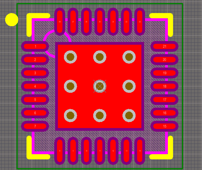
KiCad thermal pads for components like power regulators need special attention. In the footprint editor, create a large SMD pad for the thermal area. To add KiCad thermal vias, place through-hole pads with the same pad number inside the SMD pad outline; KiCad treats them as connected. Follow library conventions by adding a bottom copper pad for via relief and avoiding paste over larger vias. Name the footprint with _ThermalVias suffix for clarity.
Best Practices for Effective Heat Dissipation
Start with zone priority: higher numbers fill first, preventing overlaps on multi-zone layers. Use solid fills for maximum dissipation but switch to hatch for flexible prototypes to save copper. Always enable automatic zone refill in preferences for real-time updates during routing. For heat-heavy designs, array multiple thermal vias under pads, spacing them evenly and tenting if solder wicking is a concern.
Combine KiCad thermal relief with wider traces and inner plane layers for layered dissipation. Test spoke parameters iteratively: wider spokes improve conductivity but hinder soldering. DRC is your ally; set thermal relief violations to errors early. For hobbyist boards, prioritize hand-solderability with generous gaps around 0.2-0.3mm equivalents, adjusting via board constraints.
Avoid common errors like unfilled zones before export or ignoring pad overrides. Use net ties for grouped pads sharing zones without clearance violations. These practices align with IPC-6012 performance specs, ensuring boards withstand thermal cycling.
Troubleshooting Common Issues
If spokes don't appear, verify the pad net matches the zone and refill zones. Geometry clashes, like nearby tracks, can starve spokes; widen clearances or reroute. For custom pads, add thermal relief templates in Pad Edit Mode as lines to guide spoke placement. Vias without relief on bottom layers may complicate assembly; add a surrounding copper pad there.
DRC flags "thermal relief connection incomplete" when spoke count dips below minimum. Increase the count in Constraints or manually connect with thin tracks. Thermal vias wicking solder? Reduce via size or mask them on top. Prototype a test coupon with varied settings to dial in your process.
Conclusion
Mastering KiCad thermal relief, thermal pads, and thermal vias elevates your PCB designs from functional to reliable. By configuring zones properly, leveraging DRC, and applying best practices, hobbyists achieve excellent heat dissipation without soldering headaches. Follow structured steps on how to make thermal relief in KiCad, reference standards sparingly, and iterate with prototypes. Your boards will handle power efficiently, assemble smoothly, and perform consistently.
FAQs
Q1: What is KiCad thermal relief and when should I use it?
A1: KiCad thermal relief creates spokes between pads and copper zones for easier soldering. Use it on all power/ground pads connected to planes, especially for hand assembly. It prevents heat sinking while allowing dissipation. Set it in Zone Properties under Pad Connection. This balances reliability per industry soldering guidelines.
Q2: How do I add KiCad thermal vias to a thermal pad?
A2: In the footprint editor, place through-hole pads with the same number as the main thermal SMD pad. Position them evenly under the pad for heat transfer. Connect to inner planes via routing. Avoid paste over vias to prevent wicking. This setup enhances dissipation for power components.
Q3: Why are my thermal relief spokes missing in KiCad?
A3: Missing spokes often result from unfilled zones, net mismatches, or tight clearances. Refill zones with B, check pad nets, and run DRC. Adjust Minimum Spoke Count in Board Setup. Manual tracks fix stubborn cases. Always verify before Gerber export.
Q4: What are best practices for KiCad thermal pad design?
A4: Use large exposed pads for ICs, embed thermal vias, and apply thermal relief to surrounding zones. Ensure bottom relief for vias. Prioritize even via spacing and zone connections. Test solderability on prototypes. This optimizes heat flow without assembly issues.
References
IPC-2221A — Generic Standard on Printed Board Design. IPC, 2003
J-STD-001G — Requirements for Soldered Electrical and Electronic Assemblies. IPC, 2011
IPC-6012E — Qualification and Performance Specification for Rigid Printed Boards. IPC, 2017


