Introduction
In modern electronics, managing heat in printed circuit boards (PCBs) stands as a critical challenge for electrical engineers designing high-power density systems. Components such as power amplifiers, processors, and voltage regulators generate significant thermal loads that can degrade performance, accelerate failure mechanisms, and compromise reliability. Thermal vias and PCB thermal reliefs emerge as essential features in PCB layouts, each addressing heat dissipation from distinct angles. Thermal vias provide vertical heat pathways through the board stackup, while thermal reliefs optimize horizontal connections between pads and copper planes. Together, they form a synergistic approach to heat management, enhancing overall thermal performance without sacrificing manufacturability. This article explores PCB thermal relief with thermal vias, their combined benefits, and a thermal via design guide tailored for engineering applications.
Understanding Thermal Vias and Thermal Reliefs
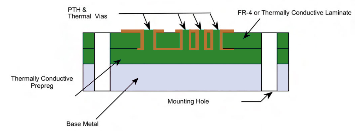
Thermal vias are plated through-holes strategically placed to conduct heat from surface-mounted components to inner copper layers or the opposite board side. These vias exploit the high thermal conductivity of copper barrel plating, acting as efficient conduits for dissipating localized hotspots. In contrast, PCB thermal reliefs consist of patterned connections, typically spokes or windows, between component pads and extensive copper pours like ground or power planes. These patterns prevent excessive heat sinking during soldering, ensuring uniform reflow while still providing a thermal path during operation. The relevance of these features intensifies in multilayer boards where heat must traverse dielectrics with lower conductivity. By integrating both, engineers achieve balanced thermal spreading, crucial for meeting performance specs in demanding environments.
Why do thermal vias and reliefs matter? Excessive junction temperatures lead to electromigration, delamination, and reduced mean time between failures (MTBF). IPC-2221 outlines guidelines for such features, emphasizing their role in conductor plane connections and via thermal management. In high-reliability sectors like automotive and aerospace, improper heat handling violates qualification standards such as IPC-6012. The synergy lies in leveraging reliefs for solder joint integrity alongside vias for bulk heat transfer, directly improving thermal performance with vias and reliefs.
Technical Principles of Heat Transfer in PCBs
Heat flow in PCBs follows Fourier's law, where flux is proportional to the temperature gradient and material conductivity. Copper exhibits around 400 W/m·K thermal conductivity, far surpassing FR-4's 0.3 W/m·K, making metal features dominant pathways. Thermal vias reduce effective thermal resistance by paralleling multiple paths vertically, with resistance scaling inversely with via count and plating thickness. For a single via, thermal resistance depends on diameter, length (board thickness), and plating; arrays compound this effect. Thermal reliefs introduce controlled constriction via spokes, typically at 45-degree angles, which throttle heat during assembly but allow conduction under bias.
The interaction between thermal vias and reliefs hinges on placement and geometry. When thermal via placement near thermal reliefs occurs, heat from a component pad flows through the relief to a plane, then funnels into adjacent vias for interlayer transfer. This minimizes lateral spreading losses in thin dielectrics. Spoke width and gap dimensions influence transient vs. steady-state performance; narrower spokes enhance assembly but increase resistance. Simulations reveal that direct connections outperform reliefs for dissipation, yet standards mandate reliefs for manufacturability. Engineers must model theta_JA (junction-to-ambient) considering convection, radiation, and conduction interplay.
Synergistic Design Strategies for Optimal Performance
Combining PCB thermal relief with thermal vias requires precise thermal via placement near thermal reliefs to maximize synergy. Position via arrays directly beneath exposed thermal pads of packages like QFNs or LQFP, with reliefs on peripheral through-hole pins connected to planes. This setup channels heat radially via reliefs into the plane, then axially through vias to sinks or chassis. Optimal via diameter balances plating uniformity and density; smaller vias (e.g., microvias in HDI) pack more densely but demand finer fabrication. Tent unused via mouths to prevent solder wicking, and consider epoxy-filled vias for enhanced conductivity and mechanical robustness.
Improving thermal performance with vias and reliefs involves stackup optimization. Connect vias to full copper pours on multiple layers, stitching with additional vias for lateral distribution. Avoid isolating vias in small islands, as this bottlenecks flow. For high-power devices, arrays of 9-25 vias under pads prove effective, spaced at 1-2 mm pitch to evade resonance in reflow. Thermal relief spoke count—often three or four—affects peak temperature rise; simulations guide trade-offs. Adherence to IPC-2221 ensures these features align with design rules for conductor widths and clearances.
A thermal via design guide starts with hotspot identification via power loss calculations (P = I2R or V·I). Place vias within the component footprint, ensuring annular rings overlap relief zones. For double-sided boards, mirror arrays top-to-bottom. In multilayer designs, stagger vias across layers to broaden the heat sink area. Verify via current capacity per IPC standards to prevent electromigration under thermal stress. Finally, incorporate ground stitching vias around the array to equalize potentials and bolster EMI immunity.
Best Practices and Troubleshooting Insights
Practical implementation demands simulation tools for iterative refinement, correlating modeled theta values with prototypes. Best practices include copper balancing across layers to symmetrize warpage and thermal expansion. During layout, prioritize via tenting on the solder side for reflow ovens per J-STD-020 guidelines on moisture sensitivity. Troubleshooting common issues starts with reflow defects: excessive relief gaps cause cold joints, while solid connects overheat barrels. Measure via plating integrity post-fabrication via cross-section analysis.
For high-frequency applications, thermal vias double as return paths, but inductance rises with length; microvias mitigate this. In troubleshooting overheating, inspect via-to-plane connections—broken pours inflate resistance. Case insight: In a power supply module, adding 16 thermal vias adjacent to relieved power pads dropped hotspot by observable margins in IR thermography, without assembly failures. Scale arrays based on power density; >5W/mm2 warrants filled vias. Validate via thermal resistance empirically using transient boundary condition measurements.
Conclusion
Thermal vias and PCB thermal reliefs together offer a powerful, synergistic approach to heat management, balancing dissipation efficacy with assembly reliability. Strategic thermal via placement near thermal reliefs optimizes paths, directly enhancing system longevity and performance. Engineers benefit from a structured thermal via design guide: array sizing, plane connectivity, and standard compliance. As power densities climb, mastering these techniques becomes indispensable for robust designs. Prioritize simulation, prototype validation, and iterative refinement to harness their full potential.
FAQs
Q1: What is the optimal thermal via placement near thermal reliefs for high-power ICs?
A1: Position via arrays centrally under thermal pads, with relief spokes linking peripheral pads to planes. This funnels heat efficiently while preserving solderability. Space vias 1-1.5 mm apart, connecting to at least two inner planes. Verify with thermal simulation to ensure uniform spreading. IPC-2221 provides foundational rules for such integrations.
Q2: How does PCB thermal relief with thermal vias improve thermal performance?
A2: Thermal reliefs provide horizontal conduction to planes, where vias enable vertical transfer, reducing junction temperatures. Relief patterns prevent soldering issues without fully blocking paths. Arrays amplify parallel conduction, lowering effective resistance. This synergy suits dense boards, outperforming isolated features. Monitor via fill for maximal gains.
Q3: What key factors define a thermal via design guide?
A3: Core elements include via diameter, count, plating thickness, and plane stitching. Tent or fill vias to block solder and boost conductivity. Align with component footprint for minimal path length. Balance density against drill feasibility. Standards like IPC-2221 guide geometries for reliability.
Q4: When should thermal reliefs be avoided in favor of direct connects with vias?
A4: Opt for direct connects under high-dissipation pads if assembly uses precise profiling, prioritizing heat flow over reflow ease. Retain reliefs for through-hole or large planes. Vias compensate by providing alternate paths. Test prototypes to confirm joint integrity.
References
IPC-2221C — Generic Standard on Printed Board Design. IPC
IPC-6012E — Qualification and Performance Specification for Rigid Printed Boards. IPC, 2018
J-STD-020E — Moisture/Reflow Sensitivity Classification of Nonhermetic Surface Mount Devices. JEDEC, 2014


