Introduction
In modern PCB design, managing heat dissipation has become critical as electronic devices pack more power into smaller spaces. Thermal vias serve as essential pathways for transferring heat away from high-power components, preventing performance degradation and extending device lifespan. Electrical engineers often encounter challenges with hotspots under components like power ICs and processors, where inadequate cooling leads to reliability issues. Understanding what is thermal via and implementing them correctly can significantly enhance overall board thermal performance. This article provides a thermal vias design guide, covering fundamentals, best practices, and applications such as via stitching on thermal pads. By following structured approaches aligned with industry standards, designers can optimize cooling without compromising electrical integrity.
What Is a Thermal Via?
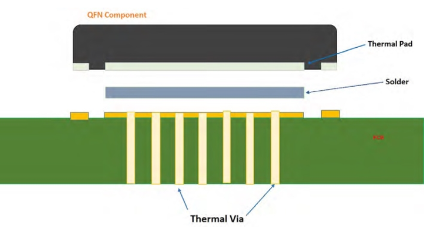
A thermal via is a plated through-hole in a PCB that facilitates heat transfer from surface-mounted components to inner layers or the opposite side of the board. These vias, typically filled or plated with copper, create low-resistance thermal paths connected to copper planes acting as heat spreaders. Unlike signal vias focused on electrical connectivity, thermal vias prioritize conduction of heat generated by active devices. They are commonly placed in arrays under thermal pads of packages like QFNs or power regulators. Electrical engineers specify thermal vias by their diameter, pitch, and connection to ground or power planes to maximize efficiency.
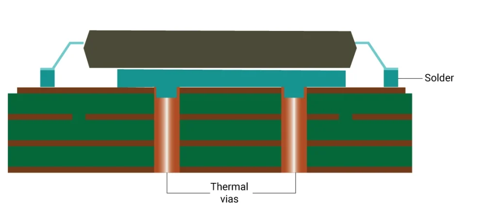
The mechanism relies on the high thermal conductivity of copper, which conducts heat far better than the FR-4 substrate material surrounding it. Heat enters the via from the component pad, travels through the barrel plating to adjacent layers, and spreads laterally via plane copper. In multilayer boards, stacking multiple inner planes connected by thermal vias forms an effective heat sink network. Designers must ensure vias do not introduce unintended electrical parasitics, such as capacitance between layers. Proper tenting or filling prevents solder wicking during assembly, maintaining thermal performance.
The Importance of Thermal Vias in PCB Design
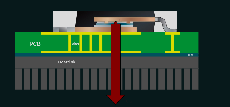
Thermal vias play a vital role in maintaining component junction temperatures within safe operating limits, especially in high-density boards. Without them, localized hotspots can cause electromigration, solder joint failures, or reduced mean time between failures. The importance of thermal vias grows with increasing power densities in applications like automotive electronics, telecommunications, and computing. They enable passive cooling strategies, reducing reliance on active heatsinks or fans that add cost and complexity. In compliance with IPC-2221 guidelines for printed board design, thermal vias help balance electrical and thermal requirements.
Effective heat spreading via thermal vias lowers the thermal resistance from junction to ambient, improving overall system reliability. Engineers observe that boards with optimized thermal vias exhibit more uniform temperature profiles across layers. This uniformity minimizes warpage risks during reflow soldering and operational thermal cycling. Moreover, thermal vias support higher current handling in power distribution networks by aiding in heat dissipation from traces. Neglecting them often leads to derating components, limiting board capabilities unnecessarily.
When to Use Thermal Vias in PCB Design
Incorporate thermal vias whenever components dissipate more than a few watts or datasheets recommend exposed pads for cooling. High-power devices such as voltage regulators, motor drivers, and RF amplifiers benefit most from these structures under their thermal pads. Use them in multilayer PCBs where inner planes provide additional spreading capacity, particularly if board thickness exceeds standard values. Single-layer or double-layer boards may require thermal vias to route heat to the bottom side for external sinks. Avoid them in low-power signal areas to prevent unnecessary via fields that could interfere with routing.
Consider environmental factors like ambient temperatures above 40 degrees Celsius or enclosed enclosures that trap heat. Thermal simulation tools reveal hotspots early, guiding when to use thermal vias in PCB design for targeted relief. In high-reliability applications, such as aerospace or medical devices, they ensure compliance with thermal management needs. Board stackup influences decisions; thicker dielectrics demand more vias to bridge layers effectively. Always evaluate trade-offs with fabrication costs and assembly yields.
Thermal Vias Design Guide
Start the thermal vias design guide by determining via dimensions based on board capabilities and component footprint. Typical diameters range from 0.2 to 0.4 mm, with pitches around 0.8 to 1.2 mm to form dense arrays without weakening the board. Connect each via directly to the thermal pad and at least one inner copper plane, preferably multiple for better spreading. Uncovered vias on the top side aid solder paste flow during reflow, but tent the bottom to avoid solder balls. Maintain aspect ratios below 10:1 for reliable plating, as per general fabrication practices.
Array configuration matters: a grid pattern under the pad maximizes coverage, with edge spacing at least twice the via diameter. For larger pads, divide into zones connected by stitching to ensure uniform heat flow. Simulate thermal performance to iterate on via count and placement before finalizing. Integrate with copper pours on all connected layers, poured to the board edge where possible for convection. Fabricators appreciate clear documentation of via tenting and filling preferences to match thermal goals.
Via filling options include conductive epoxy for enhanced conductivity or air for cost savings, depending on power levels. In high-vibration environments, filled vias reduce fatigue risks. Always verify impedance to ground planes if electrical isolation is needed. This structured approach yields predictable cooling improvements.
Via Stitching on Thermal Pads
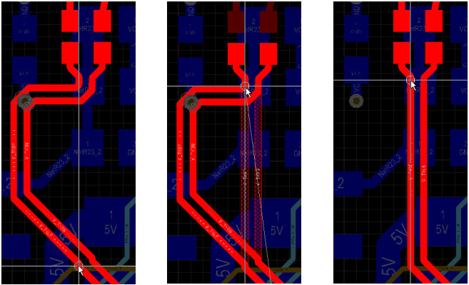
Via stitching on thermal pads involves placing multiple vias around or within the pad perimeter to tie multiple layers together, enhancing both thermal and electrical performance. This technique shorts planes across layers, reducing inductance for power delivery while spreading heat radially. Engineers apply via stitching when pad sizes exceed 5 mm squared or currents surpass 5 A, creating redundant paths. Space stitches 2 to 5 mm apart along edges, avoiding the center to preserve solder joint integrity.
The process strengthens mechanical stability under thermal expansion mismatches. Combine stitching with filled thermal vias in the pad interior for hybrid benefits. IPC-6012 performance specifications indirectly support this by emphasizing interlayer connections for reliability. In power stages, stitching prevents hotspots at pad corners. Test prototypes with infrared imaging to validate uniformity.
Stitching excels in high-frequency designs where return paths need low impedance. It complements thermal vias by providing perimeter heat escape routes. Avoid over-stitching, which raises costs without proportional gains. Layer assignment prioritizes thick copper inner layers for stitching targets.
Best Practices for Implementation
Follow a systematic workflow: identify heat sources from power budgets, model stackup thermal conductivity, then array vias iteratively. Balance via density with drill limits; excessive numbers increase fabrication time. Use ground planes as primary heat sinks, isolating signal layers. During layout, route no traces under thermal via fields to prevent shorts.
Post-layout, perform finite element analysis for junction temperatures. Collaborate with fabricators early on via plating thickness, typically 1 oz equivalent. For assembly, specify no-clean flux compatible with open vias. Monitor via reliability in thermal cycling per JEDEC standards. Document pad exposure ratios for consistent yields.
Common pitfalls include poor plane connections causing thermal bottlenecks or solder mask over vias blocking heat. Mitigate with design reviews. Scale via arrays proportionally to power dissipation for scalability.
Conclusion
Thermal vias represent a cornerstone of effective PCB thermal management, enabling engineers to harness multilayer capabilities for superior cooling. From understanding what is thermal via to mastering via stitching on thermal pads, proper implementation unlocks reliable performance in demanding designs. Adhering to guidelines ensures hotspots are tamed without electrical compromises. Prioritize simulation and prototyping to refine strategies. Ultimately, these techniques elevate board efficiency, supporting innovation in compact electronics.
FAQs
Q1: What is thermal via and how does it function in PCB heat dissipation?
A1: A thermal via is a copper-plated through-hole placed under heat-generating components to conduct heat to inner layers or the board's bottom side. It functions by providing a low-thermal-resistance path, leveraging copper's conductivity to spread heat via connected planes. This prevents junction overheating and improves reliability. Engineers use arrays for optimal performance, ensuring connections avoid signal interference.
Q2: When to use thermal vias in PCB design for high-power applications?
A2: Use thermal vias in PCB design for components exceeding 1–2 W dissipation, such as regulators or amplifiers with exposed pads. They are essential in multilayer boards to access inner planes for spreading. High ambient conditions or dense layouts demand them to maintain temperatures. Avoid in low-power areas to save routing space. Simulation identifies precise needs.
Q3: Provide a thermal vias design guide focusing on array placement.
A3: In a thermal vias design guide, select 0.3 mm diameter vias in a 1 mm pitch grid under pads, connecting to multiple planes. Tent bottom sides, leave top open for soldering. Maintain <10:1 aspect ratio for plating. Stitch edges for large pads. Verify with thermal modeling for uniformity. This yields efficient cooling.
Q4: What role does via stitching on thermal pads play in cooling?
A4: Via stitching on thermal pads uses perimeter vias to interconnect layers, enhancing heat spreading and current handling. It reduces inductance while aiding radial dissipation from hotspots. Place 2–4 mm apart along edges, combining with central thermal vias. Improves uniformity in power designs. Ensures mechanical robustness under cycling.
References
IPC-2221 — Generic Standard on Printed Board Design. IPC
IPC-6012DS — Qualification and Performance Specification for Flexible Printed Boards. IPC
JEDEC JESD51 — Thermal Test Chip Guideline for Solid State Devices. JEDEC