Introduction
Through-hole technology (THT) continues to play a vital role in high-power electronics, particularly where surface-mount devices fall short in handling extreme currents and heat. In applications such as power supplies and industrial inverters, through-hole components for power supplies provide unmatched mechanical robustness and thermal pathways that ensure long-term reliability. Engineers designing for high-current environments must prioritize through-hole design high current capabilities to prevent failures like overheating or trace delamination. This article delves into the principles of optimizing through-hole designs, focusing on electrical integrity, thermal management, and structural durability. By following established engineering practices, designers can achieve superior performance without compromising board space efficiency. Understanding these elements allows electric engineers to balance legacy THT strengths with modern demands.
Understanding Through-Hole Design in High-Power Contexts
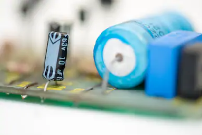
Through-hole design involves drilling holes through the PCB substrate, plating them with copper, and inserting component leads that are soldered on the opposite side. This method excels in high-power applications because the leads create robust electrical and thermal connections capable of carrying substantial currents. Unlike surface-mount technology, which relies on delicate pads, through-hole components for power supplies like electrolytic capacitors and power transistors offer larger cross-sections for current flow, reducing resistance and voltage drops. Industry relevance stems from the need for reliability in environments with vibration, thermal cycling, and high loads, common in power electronics. For instance, in motor drives or UPS systems, THT prevents solder joint fatigue that plagues SMT under mechanical stress. Electric engineers value this approach for its proven track record in mission-critical systems.
The persistence of through-hole design high current applications arises from fundamental physics: larger conductor volumes minimize I2R losses and heat generation. Standards like IPC-2221 provide guidelines for calculating current-carrying capacity based on trace width, copper thickness, and temperature rise, which directly apply to plated through-holes. Designers must consider board thickness, typically 1.6 mm or more for rigidity in power boards, to accommodate component spans without excessive stress. Hole geometry, including drill size and plating thickness, influences impedance and heat dissipation paths from component to multilayer planes. Neglecting these factors can lead to hotspots that degrade insulation or cause barrel cracking over time. Thus, THT remains indispensable for applications exceeding 10A per component.
Key Technical Principles for High-Current Handling
Effective through-hole design high current performance hinges on optimizing the plated through-hole (PTH) structure for low resistance and high mechanical strength. The copper plating in PTHs must achieve minimum thicknesses, often 25 microns or more, to handle current densities without excessive heating. Lead diameter and hole-to-lead clearance ratio affect solder fillet formation, which distributes stress evenly during thermal expansion. Engineers calculate allowable current using formulas that account for ambient temperature, airflow, and copper weight, ensuring voltage drops stay below 1% of supply rails. Multilayer boards enhance this by providing inner-layer planes that act as low-impedance returns and heat spreaders connected via the PTH. Poor design here results in electromigration, where metal atoms migrate under high current density, leading to voids and failures.
Component selection plays a pivotal role, with through-hole components for power supplies chosen for their lead materials like tinned copper or alloy steels that resist corrosion and fatigue. The annular ring around the PTH pad must extend sufficiently, typically 0.25 mm minimum, to prevent cracking during drilling or soldering. In high-power scenarios, via-in-pad configurations supplement PTHs, but THT dominates for primary power paths due to solder joint volume. Electrical simulation verifies parasitics, as inductance in long leads can cause ringing in switching circuits. Balancing these principles ensures the design withstands inrush currents and steady-state loads without derating.
Mastering Through-Hole Design Thermal Management
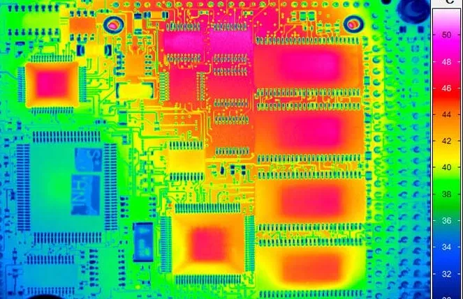
Through-hole design thermal management is critical in high-power applications, where junction temperatures in components like IGBTs or rectifiers can exceed 150°C without proper dissipation. PTHs serve as vertical heat conduits, transferring heat from component bodies through the board to inner planes or external heatsinks. Board materials with high glass transition temperatures, such as FR-4 with Tg >170°C, maintain dimensional stability under thermal stress. Copper balance between layers prevents warping, as uneven expansion coefficients cause camber in thick boards. Engineers employ thermal vias adjacent to PTHs to enhance spreading, but THT inherently outperforms SMT by allowing direct heatsink attachment via the protruding leads. Monitoring temperature rise via infrared imaging during prototyping reveals hotspots early.
Convection and conduction dominate thermal paths in through-hole assemblies. Wave soldering processes must control preheat to avoid resin degradation, per IPC-A-610 guidelines for class 3 assemblies. For forced-air cooling, component spacing allows airflow over leads, reducing thermal resistance by up to 30% compared to dense SMT layouts. In natural convection, larger PTH pads act as extended surfaces, increasing emissivity. Multilayer designs stack power and ground planes alternately, with PTHs stitching them for isothermal planes. Failure modes like solder melting or dielectric charring are mitigated by these strategies, extending mean time between failures (MTBF).
Mechanical Reliability in Through-Hole Power Designs
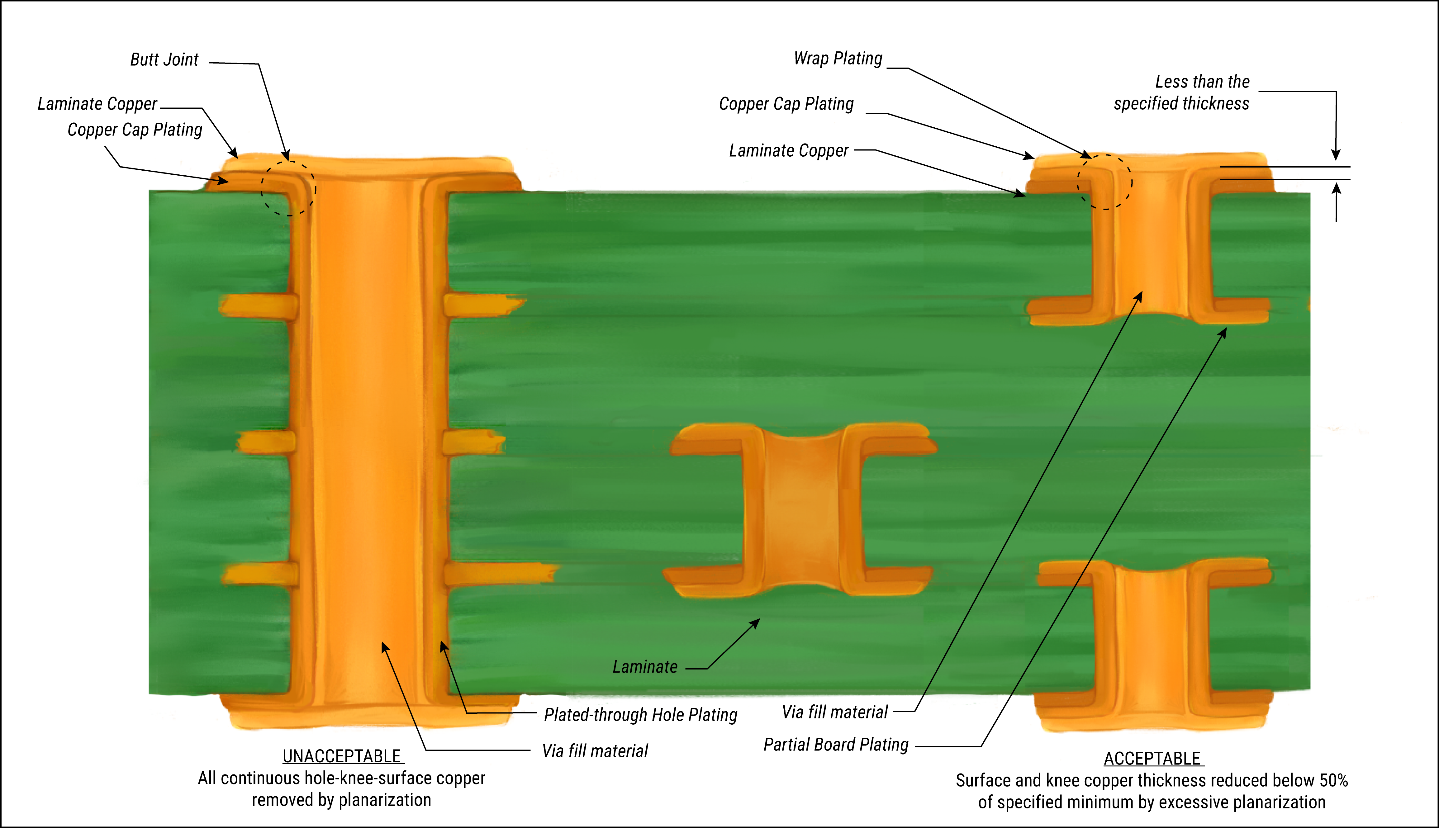
Reliability under mechanical loads sets through-hole apart, as the interleaved leads and solder barrels absorb shock and vibration better than surface pads. In high-power applications, thermal cycling induces shear stresses at the PTH-board interface, potentially causing cracks if plating adhesion is poor. Electroless nickel immersion gold (ENIG) finishes improve solderability and barrel integrity, though designers verify via cross-section analysis. Board thickness influences flexure; 2.4 mm stacks provide stiffness for heavy components without support pillars. Hole wall roughness from drilling must be minimized to ensure uniform plating, avoiding weak spots.
J-STD-001 outlines soldering criteria for high-reliability joints, emphasizing fillet height and heel formation for stress relief. In power supplies, electrolytic capacitors with THT leads benefit from this, as radial forces from bulging are distributed across the barrel. Vibration testing simulates real-world conditions, confirming no fretting at lead-hole interfaces. Combining these with edge plating or castellations enhances edge connector durability in modular power systems. Overall, mechanical optimization ensures the assembly survives drop tests and operational harmonics.
Best Practices for Optimizing Through-Hole Designs
Start with schematic-to-layout flow emphasizing power plane pours around PTHs to minimize loop inductance. Select drill sizes 0.1-0.2 mm larger than lead diameter for easy insertion and void-free soldering. For through-hole design high current, use 2 oz copper or heavier on outer layers, tapering traces to funnel current into PTHs. Simulate thermal profiles with finite element analysis to predict hotspots and adjust pad sizes accordingly. During fabrication, specify controlled impedance for signal integrity near power sections, though THT power paths prioritize DC capacity.
Assembly best practices include fixturing to prevent board sag during wave soldering, critical for double-sided THT. Post-solder inspection checks for cold joints or bridging using automated optical systems. For thermal management, integrate embedded heatsinks or thermal putty under component bodies. Prototype iterations refine hole tolerance, aiming for ±0.05 mm positional accuracy. Documentation includes Gerber files with netlist verification to catch shorts in dense power arrays. These steps yield boards ready for high-volume production with minimal rework.
Common Challenges and Troubleshooting Strategies
High-power THT boards often face warpage from asymmetric copper distribution, leading to PTH misalignment. Mitigate by adding dummy vias or balancing plane pours, verified per IPC-TM-650 methods. Solder wicking up leads reduces effective length for heatsinking; counter with flux selection and dwell time control. Barrel pullout during desoldering tests signals inadequate plating; specify 1.0 mil minimum per IPC-6012. Component lead bending during insertion stresses pads; use automated insertion tools with compliance.
Thermal runaway in clusters of through-hole components for power supplies demands zoning, separating hot spots with cutouts or slots. Humidity-induced corrosion affects tinned leads; bake-out pre-assembly removes moisture. Troubleshooting involves daisy-chain continuity tests post-assembly to isolate opens. Field failures trace to underestimating altitude derating for convection; recalculate accordingly. Proactive design reviews incorporating FMEA catch these early.
Conclusion
Optimizing through-hole design for high-power applications demands a holistic approach to electrical, thermal, and mechanical factors. By leveraging PTH strengths in through-hole design high current and through-hole design thermal management, engineers achieve reliable performance in demanding power supplies. Adhering to standards like IPC-2221 and J-STD-001 ensures compliance and repeatability. Practical best practices, from plating specs to assembly fixturing, minimize risks and enhance MTBF. As power densities rise, THT's robustness complements hybrid designs. Electric engineers can confidently deploy these strategies for next-generation systems.
FAQs
Q1: What are the key considerations for through-hole design high current in power electronics?
A1: Through-hole design high current requires thick copper plating in PTHs, typically 25-50 microns, to handle densities up to 5 A/mm2 without excessive heating. Select components with robust leads and calculate capacity using IPC-2221 formulas factoring temperature rise. Ensure annular rings exceed 0.3 mm for stress relief. Multilayer planes aid current sharing. This prevents electromigration and voltage drops in applications over 20A.
Q2: How does through-hole design thermal management differ from SMT in high-power boards?
A2: Through-hole design thermal management excels via PTH heat pipes to inner planes and direct heatsink mounting on leads. Larger solder joints enhance conduction compared to SMT's pad-limited paths. Use 2 oz copper and thermal vias for spreading. Board Tg >170°C resists delamination. This setup lowers junction temperatures by 20-40°C in power transistors.
Q3: Why choose through-hole components for power supplies over SMT equivalents?
A3: Through-hole components for power supplies offer superior mechanical anchorage against vibration and thermal cycling, ideal for capacitors and relays. Leads provide low-inductance paths for high currents. Solder volume absorbs stresses better. IPC-A-610 class 3 criteria ensure joint integrity. They simplify wave soldering for mixed assemblies. Reliability trumps density in harsh environments.
Q4: What IPC standards guide through-hole reliability in high-power applications?
A4: IPC-2221 addresses current capacity and thermal design for PTHs. IPC-6012 qualifies boards for performance under stress. J-STD-001 specifies soldering for high-reliability joints. These ensure plating adhesion and fillet quality. Cross-reference for class 3 products.
References
IPC-2221B — Generic Standard on Printed Board Design. IPC, 2012
IPC-6012E — Qualification and Performance Specification for Rigid Printed Boards. IPC, 2015
IPC-A-610F — Acceptability of Electronic Assemblies. IPC, 2017
J-STD-001G — Requirements for Soldered Electrical and Electronic Assemblies. IPC, 2011


