What Are Through-Hole Vias and Their Importance in PCBs?
If you're engaged in Printed Circuit Board (PCB) design and need to create effective connections between layers, through-hole vias represent a foundational solution. These minuscule drilled apertures, subsequently plated with conductive material, establish electrical pathways that span multiple layers within a multilayer PCB. This comprehensive guide will cover essential aspects, including various types of through-hole vias, principles of PCB layer stackup, optimal via connections, considerations for multilayer PCB design, and critical via design rules to ensure the reliability and efficiency of your boards.
Whether you're a novice designer or an experienced engineer, this resource will provide both fundamental knowledge and advanced tips for mastering through-hole vias. Let's explore how these components function and how to integrate them effectively into your designs. Through-hole vias are small holes drilled completely through a PCB, extending from the uppermost to the bottommost layer and passing through all intervening layers. These holes are then rendered conductive, typically with copper plating, to forge an electrical link between layers. They are cornerstone elements in multilayer PCB construction, facilitating the integration of intricate circuits into constrained spaces by stacking conductive layers.
Key Benefits of Utilizing Through-Hole Vias
The significance of through-hole vias lies in their capacity to simplify routing in densely populated designs. Without vias, signals and power distribution would be confined to individual layers, making the creation of compact, high-performance electronics—such as smartphones or advanced medical devices—nearly impossible. By employing through-hole vias, designers can interconnect traces across multiple layers, thereby optimizing board space and enhancing signal integrity.
● Space Optimization: They enable vertical connections, thereby freeing up horizontal surface area for component placement.
● Enhanced Signal Integrity: Properly designed vias contribute to reducing signal loss and minimizing interference.
● Robust Power Distribution: They facilitate the distribution of power and ground across different layers, which helps to mitigate electrical noise.
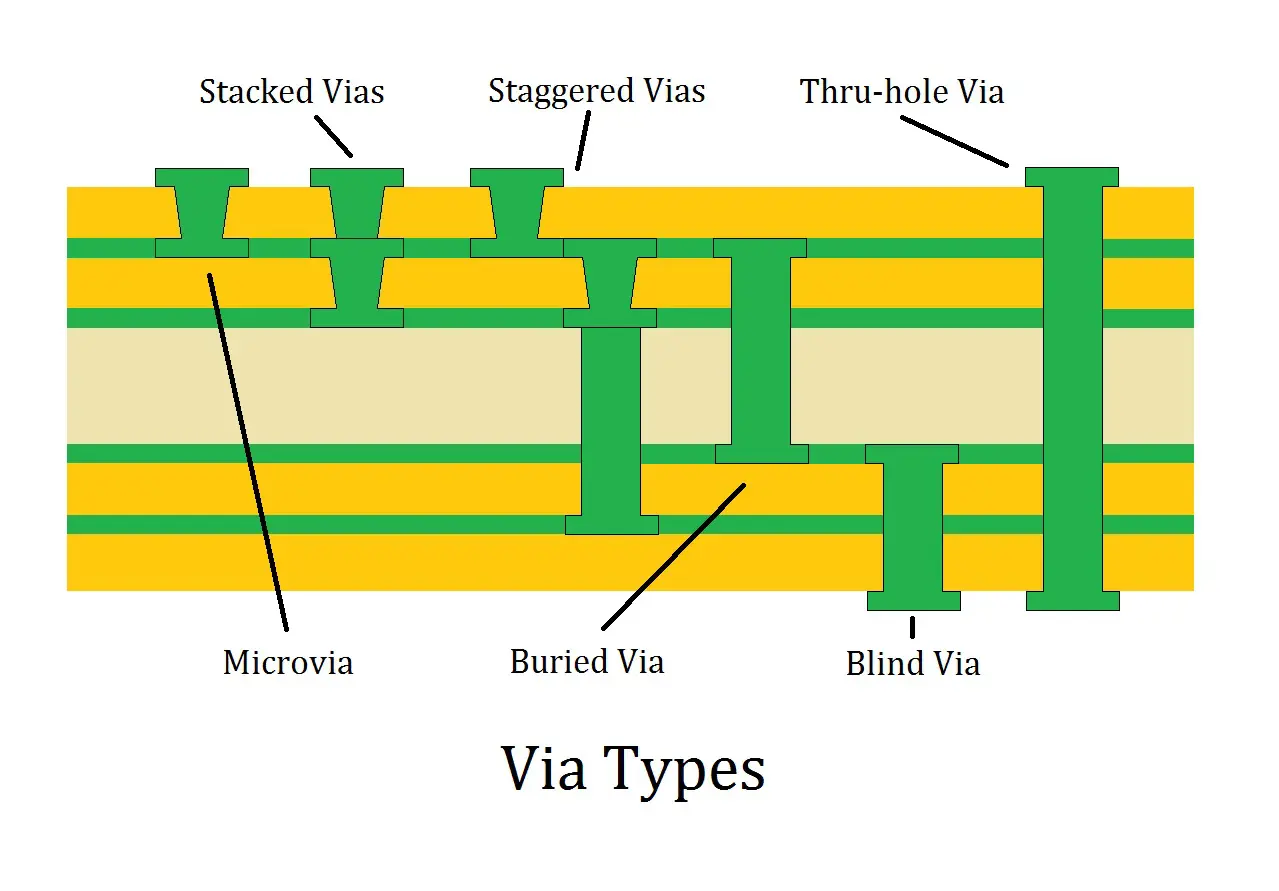
What Are the Different Types of Through-Hole Vias?
A thorough understanding of the various through-hole via types is crucial for selecting the most appropriate option for your specific PCB design. Each type serves a distinct purpose, contingent on the PCB's complexity and manufacturing capabilities. Below are the primary categories of through-hole vias commonly found in multilayer PCBs.
Common Through-Hole Via Categories
● Standard Through-Hole Vias: These are the most prevalent type, traversing all layers of the PCB. They are used for basic interlayer connections and are economically viable for the majority of designs, particularly well-suited for low-density boards where space is not a primary constraint.
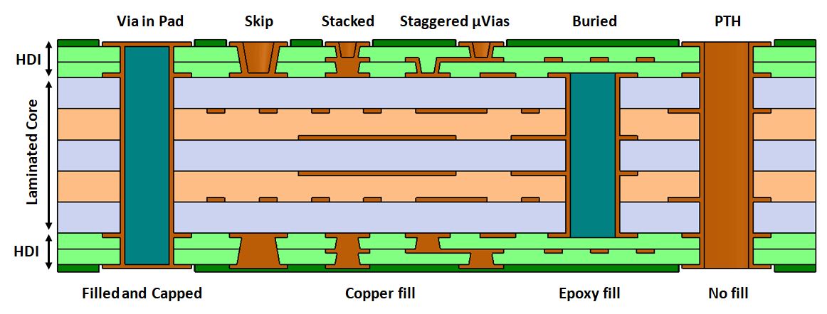
● Blind Vias: Blind vias originate from an outer layer (either top or bottom) and terminate at an internal layer, without penetrating the entire board thickness. They are particularly valuable in High-Density Interconnect PCB (HDI PCBs) designs, as they conserve space on the opposite side of the PCB. However, their manufacturing cost is higher due to the exacting precision required.
● Buried Vias: Buried vias connect only internal layers, remaining entirely hidden from the outer surfaces of the PCB. They are frequently employed in highly complex multilayer designs to maximize available surface area for component placement. Like blind vias, they incur increased manufacturing circuit board cost but are indispensable for advanced applications.
● Thermal Vias: Thermal vias are specifically engineered to conduct heat away from heat-generating components, such as power integrated circuits (ICs), directing it towards a heat sink or a ground plane. They are typically arranged in an array directly beneath a component to facilitate efficient heat transfer. For instance, a thermal via array beneath a high-power LED might consist of 0.3mm diameter vias spaced 1mm apart to effectively manage thermal output.
How Does PCB Layer Stackup Influence Via Connections?
PCB layer stackup describes the specific arrangement of conductive copper layers and insulating dielectric materials within a multilayer PCB. A thoughtfully conceived stackup is fundamental for ensuring signal integrity, efficient power distribution, and manufacturability. Through-hole vias play a pivotal role in linking these layers, and their placement must be synchronized with the overall stackup strategy.
Integrating Vias into Stackup Design
A typical 4-layer PCB stackup might comprise:
● Top Layer (Signal): Primarily for component placement and signal routing.
● Ground Plane: Crucial for noise reduction and providing a return path for high-frequency signals.
● Power Plane: Distributes stable power to various components across the board.
● Bottom Layer (Signal): Provides additional space for routing and component placement.
In more complex designs, such as 8 layers PCB, additional signal and plane layers are integrated to accommodate more intricate routing requirements. The thickness of the dielectric material between layers (often ranging from 0.1mm to 0.2mm for high-speed applications) directly impacts characteristic impedance, which must be carefully controlled for signals operating above 100 MHz. Through-hole vias serve to vertically interconnect these layers. For example, a standard via might route a signal from the top layer to the bottom layer, traversing intermediate ground and power planes. However, vias that pass through power or ground planes can inadvertently introduce undesirable parasitic capacitance or inductance, potentially affecting signal propagation speeds. To mitigate these effects, designers frequently position vias close to decoupling capacitors or employ stitching vias to robustly connect ground planes, thereby reducing loop inductance to values below 1 nanohenry (nH).
Optimizing Via Connections in Multilayer PCB Design
In multilayer PCBs, vias are far more than simple holes; they serve as critical conduits for signals, power, and ground. Inadequately designed vias can lead to signal degradation, increased electrical noise, or even complete board failure. Here’s a strategic approach to designing via connections in multilayer contexts.
Best Practices for Via Connections
● Signal Vias: These carry data between layers. For high-speed signals (exceeding 1 Gigahertz), the via’s length and diameter significantly affect its characteristic impedance. A via with a 0.25mm diameter and a 1.6mm length (typical for a standard 4-layer board) can introduce a parasitic capacitance of approximately 0.5 picofarads (pF), which is capable of distorting high-frequency signals. To minimize this, consider using smaller vias or integrating adjacent ground vias to create a controlled impedance pathway.
● Power and Ground Vias: These connect to internal power and ground planes, ensuring stable voltage levels across the PCB. For high-current ICs, it is common to use multiple vias (e.g., 4-6 vias per power pin) to effectively reduce both resistance and inductance. For a 3A current path, employing vias with a 0.3mm diameter can adequately handle the load if correctly spaced.
● Via Stitching: This technique involves strategically placing multiple vias to connect ground planes across different layers, which is highly effective in reducing electromagnetic interference (EMI). For example, positioning ground vias every 5mm along the board's edge can create an effective "fence" to contain high-frequency noise above 500 MHz.
Related Reading: The Impact of Via Design on PCB Prototyping: Minimizing Signal Loss and Maximizing Performance
What Are the Key Design Rules for Optimal Via Performance?
To guarantee both reliability and manufacturability, adherence to established via design rules is paramount. These guidelines help to strike a balance between electrical performance and manufacturing cost, while preventing issues such as signal loss or drilling inaccuracies during production.
Essential Via Design Rules
● Via Size and Aspect Ratio: The diameter and depth of a via directly influence its manufacturability. A general rule is to maintain an aspect ratio (depth-to-diameter) below 10:1 for standard through-hole vias. For a 1.6mm thick board, a via diameter of 0.2mm or larger is typically recommended. Smaller vias (e.g., 0.1mm) are technically feasible but significantly increase manufacturing costs and necessitate more advanced drilling technologies.
● Via Spacing: Vias should be spaced a minimum of 0.5mm apart (center-to-center) to prevent structural weakening of the PCB material. For high-density designs, always consult your manufacturer for their specific tighter spacing capabilities, as drilling precision can vary.
● Annular Ring Requirements: The annular ring refers to the copper pad that encircles a via. A minimum width of 0.15mm per side ensures a robust and reliable connection following the drilling process. For a 0.3mm via, the corresponding pad diameter should be at least 0.6mm to accommodate typical manufacturing tolerances.
● Via Placement Near Components: Generally, avoid placing vias directly underneath surface-mount components unless absolutely necessary, as they can interfere with the soldering process. If unavoidable, utilize tented vias (vias covered with solder mask) to prevent solder wicking, especially for vias smaller than 0.4mm in diameter.
● Thermal Via Design: For thermal vias, deploy an array with a pitch (center-to-center spacing) of 1.0mm to 1.2mm to maximize heat transfer efficiency without compromising the structural integrity of the board. Ensure these vias are robustly connected to a substantial copper plane for optimal heat dissipation.
Related Reading: Cost Effective Through Hole Via Design: Balancing Performance and Budget
Common Challenges and Solutions in Through-Hole Via Design
Designing with through-hole vias is not without its complexities. Here are some prevalent issues encountered in multilayer PCB projects and effective strategies to address them.
Troubleshooting Via Design Issues
● Challenge 1: Signal Integrity Problems: In high-speed designs, excessively long vias can act as unwanted stubs, causing signal reflections. For signals operating above 2 GHz, a via stub can resonate and significantly degrade signal quality.
○ Solution: Employ back-drilling to precisely remove the unused portions of the via barrel, thereby reducing the stub length to less than 0.2mm.
● Challenge 2: Manufacturing Limitations: Extremely small vias or those with very high aspect ratios can lead to drilling inaccuracies or plating defects during fabrication.
○ Solution: Adhere closely to manufacturer guidelines, which typically recommend via diameters no smaller than 0.2mm for cost-effective and reliable production.
● Challenge 3: Thermal Management Issues: Inadequate implementation of thermal vias can result in overheating within power-intensive designs.
○ Solution: Accurately calculate the required number of thermal vias based on the specific current demands and overall heat dissipation needs of your components. For a 5-watt component, an array of 10-15 thermal vias might be necessary to effectively manage heat.
Best Practices for Effective Through-Hole Via Implementation
To summarize, here are actionable best practices for incorporating through-hole vias into your PCB designs, ensuring optimal performance and manufacturability.
Strategic Via Design for Reliability
● Early Stackup Planning: Define your layer stackup early in the design process to strategically determine appropriate via placement and types.
● High-Speed Simulation: Utilize simulation tools to thoroughly analyze signal integrity for high-speed designs, aiming for characteristic impedance values around 50 ohms for most digital signals.
● Manufacturer Collaboration: Engage with your PCB manufacturer to confirm their specific capabilities regarding via size and spacing before finalizing your design.
● Minimize Via Count (Judiciously): Reduce the total number of vias where feasible to cut costs, but never compromise essential power or ground connections.
● Clear Documentation: Clearly document the purpose of each via (e.g., signal, power, thermal) within your design files for improved clarity during board assembly and testing.
Conclusion: Mastering Through-Hole Vias for Superior PCB Designs
Proficiency in designing with through-hole vias is an indispensable skill for any PCB designer working on multilayer boards. By comprehensively understanding the various types of through-hole vias, optimizing the PCB layer stackup, ensuring robust via connections, and diligently following established via design rules, you can create boards that are simultaneously high-performing and economically efficient. These seemingly small components form the foundational backbone of complex electronic systems, enabling everything from common consumer gadgets to advanced industrial applications.
As you integrate these principles into your next project, remember that meticulous attention to detail in via design can profoundly impact overall signal quality and board reliability. With the right approach, through-hole vias will empower you to achieve compact, highly efficient, and robust PCB designs precisely tailored to your specific requirements.


