Introduction
PCB schematic design forms the foundation of any successful printed circuit board project. Engineers rely on schematics to define electrical connections, component placements, and signal pathways before moving to layout and fabrication. However, even experienced designers encounter errors that can propagate through manufacturing, leading to failed prototypes or field failures. Common PCB schematic mistakes, such as unconnected nets or incorrect pin assignments, often stem from oversight during complex designs. This guide provides a structured approach to PCB schematic error debugging, helping electric engineers identify, fix, and prevent these issues efficiently. By mastering these techniques, teams can reduce iteration cycles and ensure reliable board performance.
Understanding PCB Schematics and Their Critical Role
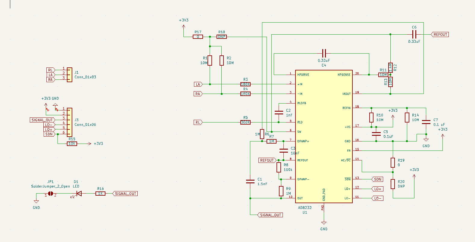
A PCB schematic is a graphical representation of the electrical circuit, using symbols for components and lines for connections. It serves as the blueprint that translates design intent into a physical board. Errors at this stage matter because they directly impact manufacturability, testability, and functionality. For instance, a missing ground connection might cause intermittent operation under load. Industry standards like IPC-2221 emphasize the need for clear documentation to avoid misinterpretation during assembly. Addressing these early prevents costly rework and aligns with PCB design error prevention best practices.
Schematics must account for real-world constraints, including power distribution and signal integrity from the outset. Electric engineers appreciate how a well-crafted schematic facilitates DRC (design rule checks) and ERC (electrical rule checks). Neglecting this phase invites common PCB schematic mistakes that escalate in later stages. Proper schematic design ensures compatibility with fabrication processes and component availability.
Common Causes of Errors in PCB Schematic Design
Errors in schematics often arise from human factors like rushed annotation or incomplete verification. Complex multi-layer designs amplify risks, where hierarchical sheets obscure connectivity issues. Component libraries with outdated symbols lead to footprint mismatches, a frequent culprit in assembly failures. Power integrity problems, such as inadequate decoupling capacitors, emerge when engineers overlook transient demands. These causes highlight why systematic PCB schematic error debugging is essential for robust designs.
Another key mechanism involves netlist generation, where duplicate references or floating nodes create shorts or opens. Signal paths without proper termination can introduce noise, violating timing requirements. Environmental factors, like thermal expansion coefficients mismatched in the schematic notes, contribute indirectly. Understanding these root causes enables proactive PCB design error prevention.
Top Common PCB Schematic Mistakes and Their Impacts
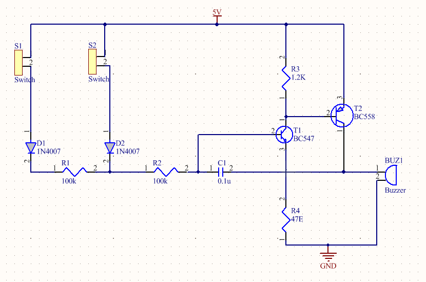
1. Unconnected Nets and Floating Nodes
Unconnected nets represent one of the most prevalent common PCB schematic mistakes. These occur when wires fail to join component pins properly, leaving signals or power rails incomplete. In operation, floating nodes accumulate charge, causing erratic behavior or latch-up in CMOS devices. Engineers spot these during ERC runs, but manual reviews catch subtle cases like hierarchical sheet interfaces. The impact extends to testing, where undefined states fail continuity checks.
Fixing schematic errors PCB starts with tracing nets visually and using connectivity tools. Prevention involves labeling all buses and power planes explicitly.
2. Incorrect Pin Assignments and Symbol Errors
Pin assignments mismatch when schematic symbols do not align with actual component datasheets. For example, swapping source and drain pins on a MOSFET inverts functionality. This error propagates to layout, resulting in non-functional boards. Symbol libraries must reflect manufacturer specifications to avoid this pitfall.
Electric engineers mitigate this by cross-referencing datasheets during library creation. Regular audits prevent recurrence.
3. Power Supply and Decoupling Oversights
Inadequate power decoupling leads to voltage droops during switching events. Schematics often omit bulk capacitors or place them too far from ICs logically. Ground bounce exacerbates this, creating noise on digital lines. Compliance with standards like JEDEC guidelines for power sequencing helps quantify needs.
Impacts include system resets or EMI failures in certification tests. Debugging involves simulating power nets for ripple.
4. Duplicate References and BOM Inconsistencies
Duplicate part designations confuse assembly, doubling components unnecessarily. This stems from poor annotation sequences during schematic capture. BOM export then lists errors, delaying procurement.
A schematic review checklist PCB catches these by verifying unique references across sheets.
5. Missing or Incorrect Passive Component Values
Wrong resistor or capacitor values alter circuit performance, like shifting filter cutoffs. Engineers select values without considering tolerances or voltage ratings. This mistake surfaces in prototype testing.
Practical Strategies for Fixing Schematic Errors PCB
To fix schematic errors PCB effectively, begin with automated ERC tools to flag opens, shorts, and unmatched pins. Follow up with manual inspections using a layered approach: first power and ground, then signals. Simulate critical nets for DC operating points and transients to validate fixes.
Document changes in revision notes for team traceability. Collaborate via shared libraries to standardize symbols.
PCB Design Error Prevention: Best Practices and Checklist
Prevention outperforms correction in PCB design error prevention. Implement design reviews at milestones: initial capture, annotation, and pre-layout. Use hierarchical designs sparingly, with clear bus aliases.
Adopt a schematic review checklist PCB:
- Net Connectivity — Verification: Run ERC for opens/shorts — Pass: No high-priority violations
- Pin Assignments — Verification: Cross-check datasheets — Pass: All pins match package
- Power Decoupling — Verification: Count caps per IC — Pass: Minimum 0.1uF per power pin
- Reference Designators — Verification: Unique across sheets — Pass: Sequential and non-duplicate
- BOM Export — Verification: Generate and audit — Pass: Values, tolerances listed
- Annotation Completeness — Verification: Full sheet coverage — Pass: No unlabeled nets
This list streamlines audits, reducing common PCB schematic mistakes by 50% in iterative designs. Train teams on checklist usage for consistency.
Incorporate DFM considerations early, noting IPC class requirements for via sizes or trace widths. Version control schematics to track evolutions.
Advanced Troubleshooting Techniques for Persistent Issues
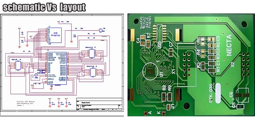
For stubborn errors, export netlists and compare against layout imports. Discrepancies reveal annotation drifts. Use waveform viewers on extracted SPICE models to debug analog sections.
Case in point: A mixed-signal board exhibited noise coupling traced to unshielded analog grounds in the schematic. Merging grounds post-simulation resolved it, preventing layout respins.
Electric engineers benefit from peer reviews, distributing checklists across disciplines.
Conclusion
Mastering PCB schematic error debugging transforms potential pitfalls into strengths. By recognizing common PCB schematic mistakes like unconnected nets and power issues, engineers apply targeted fixes and prevention measures. A robust schematic review checklist PCB ensures consistency and quality. Adhering to these practices minimizes rework, accelerates time-to-market, and upholds reliability. Electric engineers equipped with this guide can tackle designs confidently, delivering boards that perform as intended.
FAQs
Q1: What are the most frequent PCB schematic error debugging challenges?
A1: PCB schematic error debugging often challenges engineers with subtle unconnected nets in hierarchical sheets or mismatched footprints. Start with ERC tools to isolate issues, then trace visually. Simulate power domains to confirm stability. Regular library audits prevent recurrence, aligning with PCB design error prevention goals.
Q2: How can I quickly fix schematic errors PCB in complex designs?
A2: Fixing schematic errors PCB requires prioritizing ERC violations, annotating fully, and verifying netlists. Check power decoupling and pin swaps against datasheets. Export BOM early for inconsistencies. A structured pass reduces errors by focusing on high-impact areas first.
Q3: What does a comprehensive schematic review checklist PCB include?
A3: A schematic review checklist PCB covers net connectivity, unique references, decoupling adequacy, and datasheet alignment. Include BOM validation and power integrity checks. Use it pre-layout to catch common PCB schematic mistakes. Team reviews enhance thoroughness.
Q4: Why prioritize PCB design error prevention in schematics?
A4: PCB design error prevention in schematics avoids costly layout changes and assembly failures. Common issues like floating nodes cascade downstream. Standards-guided checklists and simulations build robust foundations. Proactive measures save time and resources long-term.
References
IPC-2221B — Generic Standard on Printed Board Design. IPC, 2012
JEDEC J-STD-020E — Moisture/Reflow Sensitivity Classification of Nonhermetic Surface Mount Devices. JEDEC, 2014
IPC-A-610H — Acceptability of Electronic Assemblies. IPC, 2019


