Introduction
Printed circuit boards form the backbone of modern electronics, carrying signals and power across complex assemblies. Design errors in PCBs can lead to performance failures, increased costs, and delayed production timelines. Electric engineers often encounter issues like DRC violations, ground loops, signal integrity problems, thermal hotspots, and manufacturing defects during prototyping and production. Troubleshooting these requires a systematic approach grounded in engineering principles. This guide provides practical steps for identifying and resolving these common errors, helping engineers optimize designs for reliability. By addressing root causes early, teams can reduce iterations and ensure compliance with industry benchmarks.
The Impact of PCB Design Errors on Performance and Reliability
PCB design errors compromise functionality in ways that range from subtle signal degradation to catastrophic failures. For instance, unaddressed issues can cause intermittent operation in high-speed circuits or overheating in power sections. These problems matter because they affect yield rates, field reliability, and overall system uptime. Engineers must prioritize error detection during the design phase to avoid costly rework. Understanding the mechanisms behind these errors enables proactive fixes rather than reactive patches. Ultimately, mastering troubleshooting enhances design confidence and accelerates time-to-market.
Fixing DRC Errors: Ensuring Design Rule Compliance
Design Rule Check errors flag violations of spacing, width, and layer stackup rules critical for manufacturability. Common causes include inadequate clearance between traces, vias too close to board edges, or mismatched pad sizes. These arise from oversight in layout tools or aggressive routing to fit components. To fix DRC errors, start by reviewing the design rules against fabrication capabilities, such as minimum trace width of 0.1 mm for high-density boards. Adjust violating elements systematically: widen narrow traces, relocate vias, or increase annular rings around pads. Verify fixes by rerunning DRC and simulating the updated layout for electrical performance.
Engineers should categorize DRC errors by severity, prioritizing those affecting high-voltage areas or dense signal routing. For example, insufficient via-to-via spacing can lead to shorts during etching. Iterative refinement, combined with layer-by-layer inspection, resolves most issues efficiently.
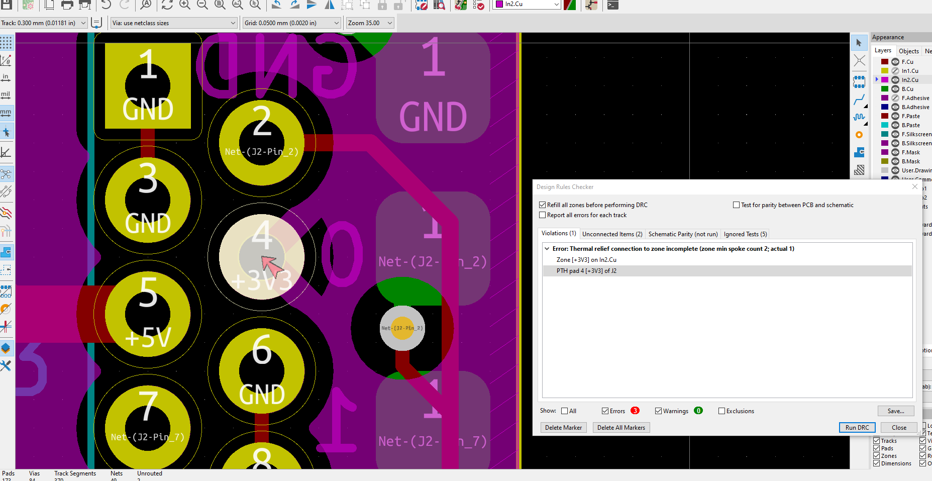
Adhering to standards like IPC-2221 helps prevent recurrence by defining generic requirements for conductor spacing and via dimensions. Document changes in a revision log to track improvements.
Identifying Ground Loops: Causes and Mitigation Strategies
Ground loops occur when multiple ground paths create unintended current flows, inducing noise in sensitive analog circuits. They stem from separate ground returns for digital and analog sections or poor star-point grounding in multi-layer boards. Symptoms include hum in audio outputs or jitter in data lines. To identify ground loops, measure voltage differences across ground planes with a high-impedance voltmeter under load conditions. Use spectrum analysis to detect low-frequency noise signatures characteristic of loops.
Mitigation involves splitting ground planes with careful stitching vias or implementing single-point grounding for low-frequency signals. Route return currents along predictable paths adjacent to signal traces to minimize loop area. In power supplies, isolate grounds with ferrite beads or optocouplers where necessary.
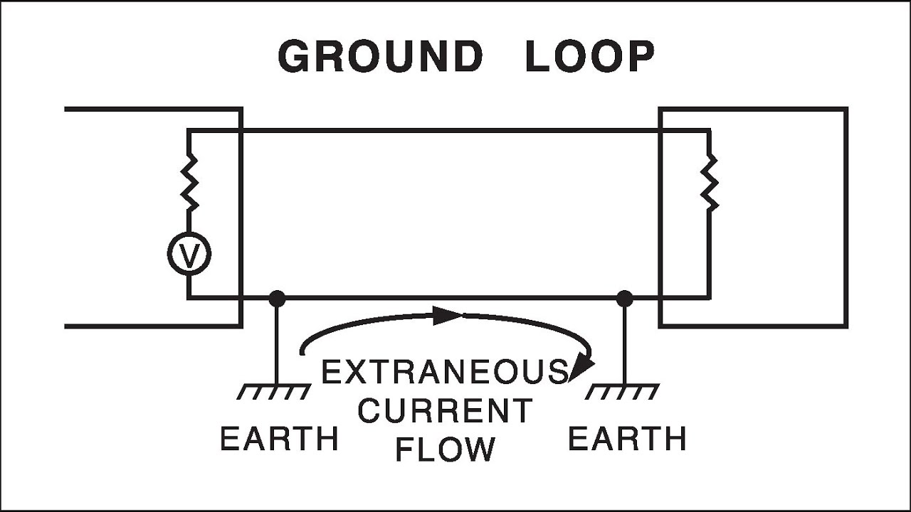
Test the design by injecting test signals and monitoring crosstalk. Consistent application of these techniques ensures clean reference potentials across the board.
Resolving Signal Integrity Issues in High-Speed Designs
Signal integrity issues, such as reflections, crosstalk, and ringing, degrade data transmission in PCBs operating above 100 MHz. Causes include impedance mismatches from varying trace widths, excessive stub lengths on vias, or capacitive coupling between adjacent lines. These manifest as eye diagram closure or bit error rates exceeding specifications. Engineers resolve them by calculating characteristic impedance using stackup parameters and matching it across the transmission line.
Implement controlled impedance routing with length-matched pairs for differential signals and serpentine tuning for skew correction. Add series resistors or AC termination to dampen reflections at source or load ends. For crosstalk, increase spacing or add ground shielding between aggressor and victim traces. Pre-layout simulations predict issues, while post-layout extraction confirms fixes.
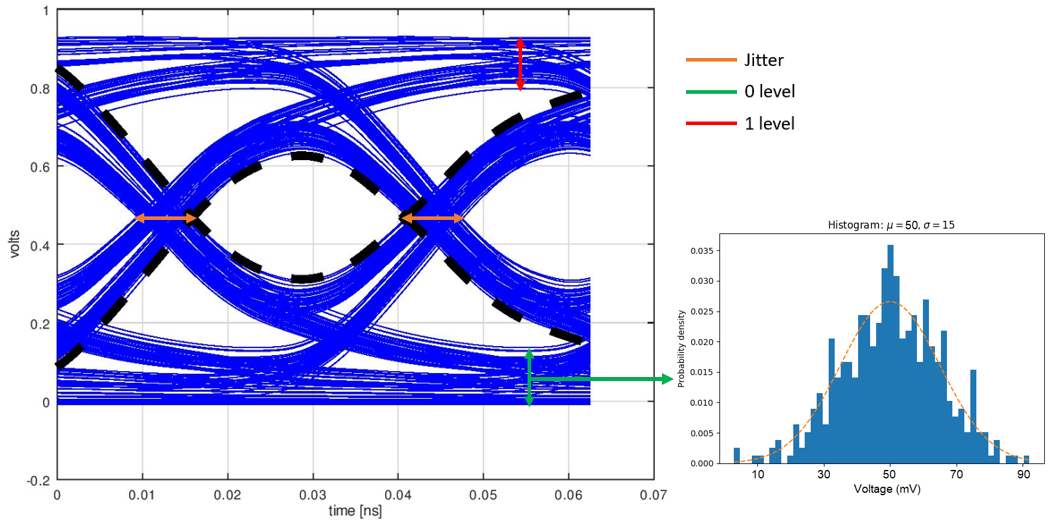
J-STD-001 provides guidelines for assembly processes that preserve signal integrity during soldering. Regular TDR measurements validate transmission line performance.
Troubleshooting Thermal Problems: Managing Heat Dissipation
Thermal problems arise from inadequate heat spreading, leading to hotspots that exceed component ratings and cause delamination. High-power devices like MOSFETs or processors generate localized heat if copper pours or vias are undersized. Contributing factors include thick dielectrics with low thermal conductivity or airflow obstruction by tall components. Identify hotspots using infrared thermography during powered operation, targeting deltas above 20°C from ambient.
Solutions focus on enhancing thermal paths: enlarge copper planes under heat sources, array thermal vias beneath pads, and select materials with higher Tg for stability. Position critical components away from board edges to leverage natural convection. Simulate thermal profiles with finite element analysis to predict junction temperatures.
IPC-2152 outlines methods for determining current-carrying capacity based on trace geometry and temperature rise. Balance thermal relief with electrical connectivity to avoid solder joint stress.
Debugging Manufacturing Defects: From Inspection to Root Cause
Manufacturing defects like opens, shorts, or warpage often trace back to design ambiguities translated poorly into fabrication. Voids in vias from plating issues or misalignment from asymmetric stackups cause intermittent failures. Debug by sectioning boards for cross-sectional microscopy or automated optical inspection for surface defects. X-ray imaging reveals inner layer shorts or barrel cracks invisible externally.
Correct designs by specifying chamfers on tabs, symmetric copper balance across layers, and bake-out for moisture control pre-lamination. Adjust drill sizes for aspect ratios under 10:1 to ensure reliable plating. Collaborate with fabricators on panelization to minimize stress during depaneling.
IPC-A-600 defines acceptability criteria for visual and dimensional attributes post-fabrication. Systematic fab DFM reviews catch potential defects early.
Best Practices for Preventing Recurring PCB Design Errors
Integrate automated checks into the workflow, including DRC, LVS, and thermal simulations from schematic capture. Maintain a design database with stackup templates tailored to signal speeds and power densities. Conduct peer reviews focusing on high-risk areas like clock distribution and power delivery networks. Prototype small panels for empirical validation before full runs.
Document lessons from past errors in a team knowledge base, emphasizing metrics like MTBF projections. Standardize via libraries and decoupling capacitor placements for consistency. These habits reduce error rates by fostering a culture of precision engineering.
Conclusion
Troubleshooting PCB design errors demands a blend of analytical tools, standards knowledge, and iterative testing. From fixing DRC errors to debugging manufacturing defects, each issue offers opportunities to refine processes. Engineers who master identifying ground loops, resolving signal integrity issues, and troubleshooting thermal problems build more robust boards. Apply these practical strategies to elevate design quality and reliability. Consistent adherence to proven methods ensures products meet performance goals without compromise.
FAQs
Q1: How do I start fixing DRC errors in a complex PCB layout?
A1: Begin by isolating violations by layer and type, such as annular ring or clearance issues. Prioritize electrical nets like power and high-speed signals. Adjust geometries incrementally while rerunning checks, and consult fabrication limits for minimum features. This structured approach, aligned with design standards, resolves most DRC errors efficiently without major redesigns.
Q2: What are the signs of ground loops and quick ways to identify them?
A2: Look for low-frequency noise, voltage offsets between grounds, or EMI susceptibility. Measure DC resistance and AC noise across paths with an oscilloscope. Identifying ground loops early prevents signal degradation; use single-point or partitioned planes for mitigation in mixed-signal boards.
Q3: How can engineers resolve signal integrity issues without redesigning the entire board?
A3: Target impedance control via trace width adjustments and via optimization. Add passive components for termination and shielding. Post-layout simulations with S-parameters verify fixes, resolving issues like crosstalk and reflections effectively for high-speed resolving signal integrity issues.
Q4: What steps help in troubleshooting thermal problems during PCB prototyping?
A4: Map temperatures with thermocouples or IR imaging under worst-case loads. Enhance dissipation through vias, pours, and heatsinks. Troubleshooting thermal problems involves iterating on stackup and component placement to keep rises within safe limits, per thermal standards.
References
IPC-2221B — Generic Standard on Printed Board Design. IPC, 2012
IPC-A-600K — Acceptability of Printed Boards. IPC, 2020
J-STD-001H — Requirements for Soldered Electrical and Electronic Assemblies. IPC, 2018
IPC-2152 — Standard for Determining Current Carrying Capacity in Printed Board Design. IPC, 2009


