Introduction
Printed circuit board stack-up design forms the foundation of reliable performance in modern electronics, especially for high-speed applications. Improper stack-up configurations often lead to issues like signal reflection, impedance mismatch, ground bounce, and EMI problems during PCB troubleshooting. Engineers frequently encounter these challenges when integrating multiple layers with varying dielectric materials and copper thicknesses. Understanding the root causes tied to stack-up decisions enables proactive fixes and reduces costly respins. This guide provides practical strategies for electric engineers to diagnose and resolve these common problems. By focusing on stack-up fundamentals, you can enhance signal integrity and overall board reliability.
What Is PCB Stack-Up and Why It Matters
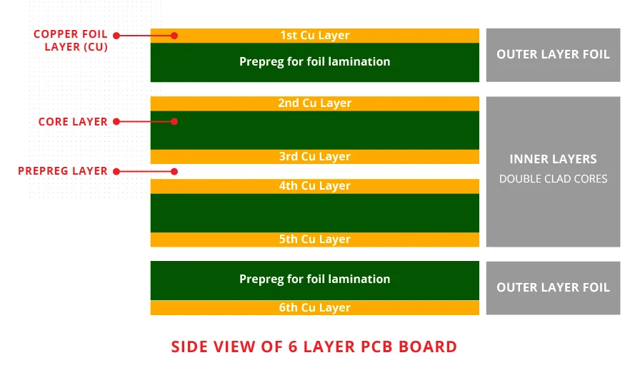
PCB stack-up refers to the precise arrangement of conductive layers, dielectric materials, prepregs, and cores in a multilayer board. It dictates electrical characteristics such as controlled impedance, crosstalk minimization, and power distribution. Poor stack-up choices disrupt signal propagation, leading to failures in high-frequency circuits. For instance, asymmetric layer sequencing can cause warpage or uneven thermal expansion, exacerbating issues like ground bounce and EMI. In electric engineering contexts, optimal stack-up ensures compliance with performance demands in telecommunications, automotive, and computing systems. Mastering stack-up directly impacts product yield and longevity.
Common Causes of PCB Stack-Up Problems
Stack-up problems arise primarily from imbalances in layer symmetry, dielectric thickness variations, and inadequate plane allocation. Signal reflection occurs when trace impedance deviates from driver and receiver expectations due to inconsistent dielectric heights between signal and reference planes. Impedance mismatch stems from manufacturing tolerances in material properties or copper etching inconsistencies across layers. Ground bounce manifests as voltage fluctuations on power planes from simultaneous switching noise, amplified by thin or segmented ground layers in the stack-up. EMI issues emerge from unshielded signal returns or poor interplane capacitance, allowing radiated emissions to escape. These mechanisms interconnect, making comprehensive PCB troubleshooting essential.
Signal Reflection and Impedance Mismatch in Stack-Ups
Signal reflection in PCB stack-ups happens at discontinuities where characteristic impedance changes abruptly, such as at vias or layer transitions. Engineers calculate impedance using formulas involving trace width, dielectric constant, and separation to ground or power planes. In asymmetric stack-ups, varying prepreg thicknesses create mismatches, reflecting energy back to the source and distorting waveforms. During PCB troubleshooting, time-domain reflectometry reveals these reflections as voltage spikes on traces. Impedance mismatch not only degrades eye diagrams but also increases bit error rates in serial links. Consistent stack-up planning with uniform dielectric stacks prevents these reflections.
To troubleshoot impedance mismatch, measure fabricated boards with a vector network analyzer comparing designed versus actual values. Stack-up errors often trace to core-prepreg combinations with differing coefficients of thermal expansion. Reference IPC-2221 for guidelines on controlled impedance design in multilayer boards. Symmetric stack-ups around the neutral axis minimize such discrepancies. Simulations prior to fabrication validate stack-up integrity against target impedances.
Ground Bounce: Stack-Up Contributions and Fixes
Ground bounce arises from inductive paths in power delivery networks, worsened by stack-up configurations lacking dedicated ground planes adjacent to signals. In dense designs, splitting ground planes or placing signals far from references induces loop inductance, causing simultaneous switching currents to generate voltage overshoots. This couples noise into adjacent traces, mimicking crosstalk during operation. PCB troubleshooting involves probing power rails with high-bandwidth oscilloscopes to capture bounce amplitudes. Stack-up remedies include dedicating inner layers as solid ground planes to shorten return paths. Increasing plane capacitance through thinner dielectrics between power and ground layers dampens these transients.
Practical mitigation starts with stripline routing where signals sandwich between planes, reducing inductance compared to microstrip. During design reviews, verify stack-up symmetry to avoid warpage that lifts planes from signals. J-STD-001 outlines soldering and assembly practices that preserve stack-up integrity post-fabrication. Engineers should allocate at least two ground planes in eight-layer stack-ups for high-speed signals. Post-assembly tests confirm bounce levels below acceptable thresholds for the application.
EMI Issues Stemming from Stack-Up Design
Electromagnetic interference in PCBs originates from stack-up flaws like insufficient shielding or imbalanced reference planes, allowing differential mode currents to radiate. EMI issues intensify when signal layers lack immediate ground references, creating long loop areas for magnetic fields. Poor interplane spacing reduces capacitive coupling, failing to shunt high-frequency noise to ground. In PCB troubleshooting, near-field probes map emission hotspots correlating to stack-up weak points. Compliance testing per IEC standards highlights radiated emissions from edge vias or unterminated traces. Optimized stack-ups embed signals within ground cages to contain fields.
Best practices include alternating signal and plane layers to form Faraday-like shielding. Thicker coppers on planes lower resistance, aiding noise return. During layout, avoid splitting planes under high-speed signals to maintain continuous low-impedance paths. EMI troubleshooting benefits from 3D field solvers modeling stack-up effects pre-prototype. Fabricated boards require shielding cans only if stack-up alone insufficient.
Practical Troubleshooting Workflow for Stack-Up Problems
Effective PCB troubleshooting begins with design verification using stack-up calculators to predict impedance and plane resonance. Fabricate test coupons alongside production panels for TDR and cross-section analysis. Visual inspections reveal delamination or asymmetry from stack-up stresses. For signal reflection, correlate simulation with measurements; adjust prepreg schedules iteratively. Ground bounce diagnostics employ power integrity tools assessing PDN impedance profiles. EMI scans guide plane stitching via additions.
Cross-sectioning exposes layer alignments, confirming dielectric thicknesses match specs. Warpage checks using shadow moire interferometry link to asymmetric stacks. Iterate stack-ups with manufacturer input on material sets. Document deviations for root cause analysis.
Best Practices for Robust Stack-Up Design
Adopt symmetric stack-ups with equal dielectric builds above and below the center to combat warpage. Pair high-speed signals with adjacent planes for 50-ohm single-ended or 100-ohm differential impedances. Use low-loss dielectrics for RF layers, transitioning to standard FR-4 cost-effectively. Allocate 20-30% of layers to power/ground for integrity. Blind/buried vias reduce stub effects in dense stack-ups.
Thermal management integrates via stitching and thicker planes. Validate with hyperlynx-like simulations before tape-out. IPC-A-600 provides acceptability criteria for fabricated stack-ups. Field testing refines designs iteratively.
Real-World Troubleshooting Insights
Consider a 12-layer board exhibiting signal reflection post-assembly. TDR traces showed 75-ohm jumps on intended 50-ohm lines due to thin prepreg under signals. Reformulating the stack-up with uniform 2116 prepregs resolved mismatches. Ground bounce in a DDR memory interface traced to split planes; merging into full sheets eliminated overshoots. EMI failures from edge launches fixed by guard traces and plane extensions. These cases underscore stack-up's pivotal role in PCB troubleshooting.
Conclusion
Mastering PCB stack-up troubleshooting addresses core issues like signal reflection, impedance mismatch, ground bounce, and EMI through systematic diagnosis and redesign. Electric engineers benefit from symmetric builds, plane dedication, and verification tools. Adhering to standards ensures reliability across applications. Proactive stack-up optimization minimizes respins and boosts performance. Implement these practices for resilient high-speed boards.
FAQs
Q1: How do you identify signal reflection during PCB troubleshooting?
A1: Signal reflection appears as voltage ringing on oscilloscope eye patterns or TDR waveforms indicating impedance discontinuities. Check stack-up for consistent dielectric thicknesses between signal and plane layers. Measure characteristic impedance and compare to design targets. Adjust prepreg counts if mismatches exceed 10%. This approach restores clean signal propagation.
Q2: What causes ground bounce in PCB stack-ups?
A2: Ground bounce results from high inductance in power/ground return paths during simultaneous switching. Stack-ups lacking adjacent planes amplify loop areas. Dedicate inner layers as unbroken grounds to lower impedance. Verify with PDN analysis tools pre-layout. Proper stack-up reduces bounce, ensuring stable logic levels.
Q3: How to mitigate impedance mismatch in multilayer PCBs?
A3: Impedance mismatch stems from varying trace-to-plane spacing in stack-ups. Use field solvers to optimize widths and dielectrics for target values. Symmetric builds maintain uniformity. Test coupons confirm fabrication accuracy. Consistent practices prevent signal degradation.
Q4: What stack-up strategies reduce EMI issues?
A4: EMI issues lessen with signals embedded between ground planes forming shields. Alternate layers and stitch planes to block fields. Minimize loop areas via short references. Near-field scans during troubleshooting pinpoint fixes. Robust stack-ups achieve compliance without add-ons.
References
IPC-2221B — Generic Standard on Printed Board Design. IPC, 2009
IPC-A-600K — Acceptability of Printed Boards. IPC, 2020
J-STD-001H — Requirements for Soldered Electrical and Electronic Assemblies. IPC, 2018


