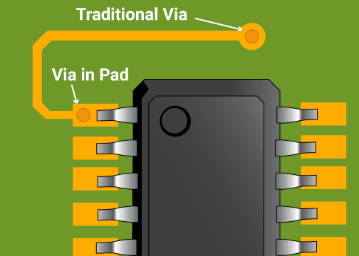
Understanding Via-in-Pad Technology in Modern PCB Design
Via-in-pad technology is a sophisticated PCB design technique that involves placing a via—a small, plated hole connecting different layers of a circuit board—directly within the solder pad of a surface-mount component. This method is particularly prevalent in high-density interconnect (HDI) designs and fine-pitch components like Ball Grid Arrays (BGAs), where board space is at a premium. By utilizing via-in-pad, designers can significantly reduce routing congestion and shorten signal paths, leading to a more compact board layout.
Beyond space efficiency, this technology also offers performance benefits, such as reduced inductance (often below 0.5 nH, compared to 1-2 nH for conventional vias) and improved thermal management. However, these advantages come with a unique set of challenges during both the manufacturing and assembly processes. Addressing these challenges is crucial for ensuring the long-term reliability and performance of the PCB.
Common Challenges Encountered with Via-in-Pad Designs
Despite its benefits, via-in-pad technology frequently presents several issues during the manufacturing and assembly stages. Understanding these problems and their root causes is the first step toward effective troubleshooting and prevention.
Via-in-Pad Solder Wicking
Via-in-pad solder wicking occurs when molten solder, during the reflow soldering process, flows down into an open or improperly sealed via. This migration of solder away from the component pad leaves insufficient solder to form a robust electrical and mechanical connection, often resulting in weak, incomplete, or open circuits.
This issue typically arises from unfilled or inadequately filled vias that provide an escape route for the solder. An excessive via diameter (e.g., larger than 0.3 mm for a 0.5 mm pad) also increases the likelihood of solder draining into the hole. Furthermore, inadequate stencil design or insufficient solder paste volume on the pad can fail to compensate for the potential loss of solder into the via, exacerbating the problem.
Via-in-Pad Solder Voids
Via-in-pad solder voids are internal air pockets or gaps that form within the solder joint. These voids are frequently caused by the outgassing of trapped moisture or air from within the via or surrounding materials during the rapid heating of the reflow process. Such voids weaken the solder joint's mechanical integrity and can significantly impair both its thermal and electrical conductivity, leading to localized hotspots or increased resistance.
The primary culprits include moisture trapped within the via barrel or the PCB's dielectric materials, which vaporizes and creates bubbles during reflow. Poor via filling or plugging techniques can also leave empty spaces where air can become entrapped. Additionally, inconsistent reflow profiles, particularly those with insufficient peak temperatures (e.g., below 240°C for lead-free solder), might prevent the solder from fully coalescing and allowing gases to escape before solidification.
Via-in-Pad Reliability Concerns
Via-in-pad reliability issues refer to long-term performance degradation or failure, such as the formation of cracks in solder joints or delamination within the via structure itself. These problems often manifest under prolonged thermal cycling, mechanical stress (like vibration or shock), or during the device's operational lifespan.
Root causes include a thermal expansion mismatch between the copper of the via and the surrounding PCB substrate (e.g., copper's CTE of 17 ppm/°C versus FR-4's 50-70 ppm/°C), which induces stress during temperature fluctuations. Solder joints weakened by prior wicking or voids are inherently less robust and more prone to cracking under stress. Moreover, poor via plating or filling can introduce internal defects that propagate and worsen over time, leading to eventual electrical or mechanical failure.
Via-in-Pad Manufacturing Defects
Via-in-pad manufacturing defects encompass a range of issues introduced during the PCB fabrication process, such as incomplete via filling, exposed copper within the via, or misalignment of the via relative to its pad. These defects can compromise the structural and electrical integrity of the board, affecting subsequent assembly stages and long-term operation.
Causes often stem from inconsistent via plugging processes, where low-quality resin or solder mask materials, or improper application techniques, result in voids, cracks, or insufficient sealing of the via. Drilling inaccuracies during fabrication (e.g., tolerances exceeding ±0.05 mm) can lead to misaligned vias, impacting pad integrity. Furthermore, insufficient copper plating thickness (below 25 μm) within the via barrel creates weak connections that are highly susceptible to fracture under thermal or mechanical stress.
Practical Solutions for Via-in-Pad Issues
Effectively troubleshooting and preventing via-in-pad issues requires a multi-faceted approach involving careful design, optimized manufacturing processes, and rigorous inspection.
Preventing Solder Wicking
To effectively combat solder wicking, the primary strategy is to prevent molten solder from flowing into the via. This is achieved by ensuring all vias are filled with a conductive or non-conductive material, such as epoxy resin, prior to soldering. Conductive fills can additionally enhance thermal and electrical performance, often achieving resistance below 10 mΩ per via. After filling, the via should be capped with a thin layer of copper or solder mask (a process known as "via-in-pad plated over"), which effectively blocks solder from entering. This method has become an industry standard. Additionally, optimizing the stencil design by increasing solder paste volume on pads with vias by 10-20% helps compensate for potential solder loss. For example, a 0.5 mm pad might use a stencil aperture of 0.55-0.6 mm. Finally, reducing via size (e.g., to 0.2-0.3 mm diameter) can minimize solder flow, though designers should confirm manufacturing capabilities for smaller via tolerances.
Mitigating Solder Voids
Minimizing solder voids focuses on eliminating sources of trapped gases and optimizing the reflow process. Pre-baking the PCB at 120°C for 2-4 hours before assembly is crucial to remove any absorbed moisture, especially for boards stored in humid environments (above 60% RH). Ensuring proper via filling with resin or conductive paste eliminates air pockets that could outgas during reflow. An adjusted reflow profile with a gradual ramp-up rate (1-3°C per second) and a peak temperature of 240-250°C (for lead-free solder) allows sufficient time for any remaining gases to escape before the solder fully solidifies. Post-assembly, X-ray inspection (2D or 3D) is vital for detecting voids. While IPC-A-610 standards may accept up to 25% voiding for Class 2 products, aiming for less than 10% is recommended for high-reliability applications.
Enhancing Reliability
To address via-in-pad reliability issues, focus on material compatibility and robust joint formation. Selecting compatible materials for the PCB substrate—such as high Tg PCB laminates or high-Tg FR-4 with a coefficient of thermal expansion (CTE) closer to copper (around 40–50 ppm/°C)—significantly reduces stress during thermal cycling (typically −40°C to 85°C). By preventing wicking and voids, you inherently reinforce solder joints, making them more resilient to mechanical stresses like vibration (as tested at 10-55 Hz per IPC standards). Thicker via barrel plating (at least 25 μm) is essential to prevent cracks under stress; thinner plating can lead to open circuits after few thermal cycles. Additionally, rigorous reliability testing, including thermal cycling (e.g., 1000 cycles between -40°C and 125°C) and drop tests, simulates real-world conditions. Microsection analysis can then be used to identify internal defects like cracks or delamination.
Correcting Manufacturing Defects
Preventing via-in-pad manufacturing defects requires clear specifications and stringent quality control. Clearly specify the via filling process (conductive paste, epoxy, or solder mask) in your design files, including details on capping to prevent exposed copper. Set tight tolerances with your manufacturer for drilling accuracy, ideally within ±0.05 mm, as misalignment can shift pads by 0.1 mm or more, causing assembly issues. Implement Automated Optical Inspection (AOI) during fabrication to detect defects like incomplete filling or exposed copper, followed by electrical testing to confirm via continuity (resistance below 10 mΩ). Adhere strictly to Design for Manufacturability (DFM) guidelines, such as maintaining a minimum annular ring of 0.1 mm around vias, to ensure proper pad integrity throughout the drilling and plating processes.
Best Practices for Proactive Via-in-Pad Design
Beyond addressing specific problems, integrating proactive best practices into the initial design phase can prevent many via-in-pad issues from ever occurring, leading to more robust and reliable PCBs.
Strategic Design and Collaboration
It's wise to limit via-in-pad usage to instances where it is truly necessary, such as for fine-pitch components (below 0.5 mm pitch) or in high-density interconnect (HDI) designs. For larger components, traditional vias placed outside the pads are generally more reliable and easier to manufacture. Early collaboration with your large PCB manufacturer is paramount; share your design files during the planning stage to confirm their specific capabilities regarding via filling, plating, and achievable tolerances. This preemptive communication can prevent unforeseen manufacturing hurdles. For high-speed designs operating above 1 GHz, simulate signal integrity thoroughly using specialized tools to ensure that via-in-pad placement does not inadvertently introduce signal reflections, impedance discontinuities, or crosstalk. Finally, meticulous documentation is critical. Include clear and detailed notes in your Gerber files and Bill of Materials (BOM) regarding all via treatments (e.g., "fill and cap all vias under BGA pads") to eliminate any ambiguity and prevent miscommunication during the fabrication and assembly processes.
Conclusion: Building Reliable PCBs with Via-in-Pad Technology
Via-in-pad technology offers significant advantages for creating compact, high-performance PCB designs, but its successful implementation hinges on a meticulous attention to detail. By thoroughly understanding the root causes of common pitfalls—such as via-in-pad solder wicking, via-in-pad solder voids, via-in-pad reliability issues, and via-in-pad manufacturing defects—and by diligently applying the comprehensive troubleshooting and preventive measures outlined in this guide, you can achieve remarkably robust and dependable designs that consistently meet your project's exacting goals.
Every step, from optimizing solder paste application and ensuring complete via filling to conducting rigorous inspections and implementing strategic design practices, plays a crucial role in the overall success and longevity of your PCB. By integrating these best practices into your engineering workflow, you will be exceptionally well-equipped to navigate and conquer the complexities of via-in-pad technology. Together, let's strive to build superior circuit boards that perform flawlessly in demanding applications.


