Introduction
High-speed printed circuit boards handle data rates exceeding several gigabits per second, making signal integrity a critical concern for reliable operation. Engineers encounter challenges such as signal reflection, crosstalk, and impedance mismatch that can degrade performance and cause system failures. Effective high-speed PCB signal integrity troubleshooting requires understanding root causes and applying targeted diagnostic tools like TDR and eye diagrams. This guide provides practical steps for analysis and resolution, drawing on established engineering principles. By addressing these issues systematically, designers can ensure robust signal transmission in demanding applications.
What Is Signal Integrity and Why It Matters in High-Speed PCBs
Signal integrity refers to the preservation of electrical signal quality from source to receiver without distortion or loss. In high-speed PCBs, signals propagate as transmission lines where wavelength approaches trace lengths, leading to wave effects like reflections and coupling. Poor signal integrity manifests as bit errors, increased jitter, or electromagnetic interference, compromising overall system reliability. As data rates climb beyond 10 Gbps, these issues intensify, affecting sectors like telecommunications and computing. Troubleshooting signal integrity early prevents costly respins and ensures compliance with performance specifications. Engineers must prioritize it to meet rising demands for faster, denser interconnects.
Common Causes of Signal Integrity Issues
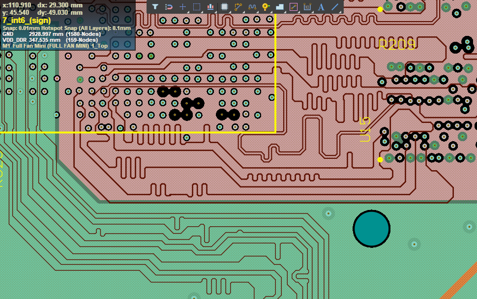
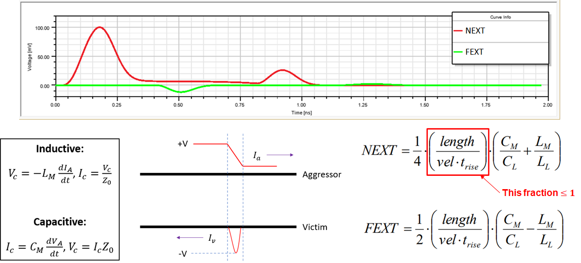
Impedance mismatch occurs when trace characteristic impedance deviates from driver or receiver expectations, primarily due to inconsistent stackup, varying trace widths, or abrupt geometry changes. This mismatch generates reflections that superimpose on the original signal, causing overshoot, ringing, or attenuation. Crosstalk arises from electromagnetic coupling between adjacent traces, with near-end crosstalk dominating capacitive effects and far-end from inductive coupling. Vias, bends, and plane splits exacerbate these problems by introducing discontinuities. Fabrication tolerances in dielectric thickness or copper roughness further contribute to variations. Understanding these mechanisms guides precise high-speed PCB signal integrity troubleshooting.
Signal reflection follows the reflection coefficient formula, where mismatch voltage reflects back, potentially doubling amplitude if unterminated. In uncontrolled environments, multiple reflections create standing waves that distort timing and amplitude margins. Crosstalk magnitude depends on coupling length, spacing, and rise time, often scaling inversely with separation. Engineers observe these in simulations before fabrication to predict behaviors accurately.
Diagnostic Tools for Signal Integrity Analysis
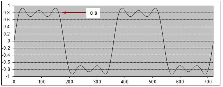
Time Domain Reflectometry (TDR) measures impedance profile along traces by sending a step signal and analyzing reflections. Discontinuities appear as impedance steps on the TDR trace, pinpointing locations with millimeter resolution. For high-speed PCB signal integrity troubleshooting, TDR excels at identifying via stubs, pad mismatches, or etch variations. Eye diagrams overlay multiple bit transitions to visualize signal quality, revealing jitter, eye height, and width critical for bit error rate estimation. A closed eye indicates issues like crosstalk or ISI, while open eyes confirm margins. Combining these with PCB testing via oscilloscopes provides comprehensive signal integrity analysis.
Simulation tools model pre-layout scenarios, predicting reflection, crosstalk, and insertion loss using S-parameters. Post-fabrication validation correlates measurements to simulations for root cause isolation. Frequency domain analysis via vector network analyzers complements TDR for broadband characterization. Engineers iterate between simulation and testing to refine designs efficiently.
Best Practices to Mitigate Signal Integrity Problems
Achieve controlled impedance through stackup optimization, selecting dielectrics with low loss tangent and precise trace geometries per design guidelines in IPC-2221C. Maintain 50-ohm single-ended or 100-ohm differential impedance with symmetric routing and ground reference planes adjacent to signal layers. Reduce crosstalk by enforcing 3W spacing between traces, where W is trace width, and shielding critical lines with ground traces. Minimize via count, use back-drilling for stubs, and avoid right-angle bends, favoring 45-degree miters. Length matching within 5% of bit time ensures timing alignment, preventing skew-induced ISI.
Proper termination, series or parallel resistors, absorbs reflections at source or load. Solid reference planes without splits under high-speed nets provide return paths and suppress radiation. IPC-6012F outlines performance specs ensuring fabricated boards meet these electrical targets. Layer sequencing with signal-ground-signal stacking isolates coupling effectively.
Step-by-Step Troubleshooting Workflow
Begin with simulation-based signal integrity analysis to baseline expected performance against specs. Fabricate prototypes and perform TDR scans on all critical nets to map impedance variations. Correlate TDR anomalies with layout reviews, focusing on vias and transitions. Acquire eye diagrams at receiver ends under worst-case conditions like maximum data rate and temperature. Quantify crosstalk by injecting aggressor signals and measuring victim perturbation. If issues persist, dissect via cross-sectioning or S-parameter extraction for deeper insights.
Iterate fixes like rerouting or adding stitching vias, reverifying with PCB testing. Document margins against budgets for reflections under 5%, crosstalk below -30 dB. This structured approach resolves most high-speed PCB signal integrity troubleshooting challenges efficiently.
Advanced Considerations in Signal Integrity
Dielectric losses from skin effect and material dissipation increase with frequency, narrowing eyes progressively. Rough copper surfaces elevate effective loss, necessitating smoother foils for >20 Gbps. Pre-emphasis and equalization compensate channel losses dynamically. Multi-layer effects like mode conversion in differentials demand tight symmetry. Integrating these refines signal integrity analysis for next-gen speeds.
Conclusion
Troubleshooting signal integrity issues in high-speed PCBs demands a blend of simulation, precise measurements like TDR and eye diagrams, and adherence to best practices. Addressing impedance mismatch, reflections, and crosstalk systematically ensures reliable performance. Engineers benefit from proactive design per industry standards, minimizing post-fabrication surprises. Implementing these strategies optimizes PCB testing outcomes and accelerates product deployment. Continuous validation maintains integrity across design cycles.
FAQs
Q1: What role does TDR play in high-speed PCB signal integrity troubleshooting?
A1: TDR sends fast rise-time pulses to detect impedance discontinuities along traces, revealing reflections from mismatches or vias. It localizes issues with high resolution, guiding targeted fixes like back-drilling. Combined with layout data, TDR facilitates rapid signal integrity analysis without full system assembly. This tool proves essential for validating controlled impedance post-fabrication.
Q2: How do eye diagrams aid in signal integrity analysis?
A2: Eye diagrams superimpose signal transitions to assess quality metrics like height, width, and jitter. Closed eyes signal problems such as crosstalk or ringing from impedance mismatch. Engineers use them during PCB testing to quantify margins against bit error rates. Analysis helps prioritize interventions in high-speed designs effectively.
Q3: What are common causes of crosstalk in high-speed PCBs?
A3: Crosstalk stems from capacitive and inductive coupling between parallel traces, amplified by close spacing and long coupling lengths. Fast rise times exacerbate near-end and far-end effects. Mitigation involves wider spacing and ground shielding. Simulation predicts levels before PCB testing confirms reductions.
Q4: Why is simulation important in high-speed PCB signal integrity troubleshooting?
A4: Simulation predicts reflections, crosstalk, and losses pre-layout, allowing design iterations without prototypes. It models stackup and routing impacts accurately. Post-fabrication correlation refines models for future use. This front-loading saves time in signal integrity analysis.
References
IPC-2221C — Generic Standard on Printed Board Design. IPC, 2023
IPC-6012F — Qualification and Performance Specification for Rigid Printed Boards. IPC, 2023


