Introduction
Printed Circuit Boards, or PCBs, form the backbone of modern electronics, providing a structured platform for components to connect and function. For electronic hobbyists, understanding PCB basics is essential to design and build reliable projects. This guide focuses on core elements such as layers, traces, and vias, breaking down complex concepts into simple terms. Whether you're exploring single layer versus double layer PCB designs or learning basic PCB terminology, this article offers a clear path forward. By grasping these fundamentals, hobbyists can create efficient circuits and avoid common pitfalls. Let's dive into the structure, materials, and design principles that define PCBs, ensuring you have the knowledge to advance your skills in this exciting field.
What Is a PCB and Why It Matters
A PCB is a flat board made of insulating and conductive materials that supports and connects electronic components. It serves as the foundation for devices ranging from simple LED circuits to complex microcontrollers. For hobbyists, PCBs matter because they simplify assembly, reduce wiring errors, and improve durability compared to breadboards or point-to-point wiring. Understanding PCB layers, traces, and vias allows better control over circuit performance and space efficiency. Without this knowledge, designs may suffer from signal issues or manufacturing flaws. PCBs also enable scalability, letting hobbyists transition from prototypes to PCB mass production. By mastering these basics, you ensure your projects are both functional and reliable, paving the way for more advanced electronic creations.
PCB Layers Explained for Beginners
PCBs are constructed in layers, each serving a specific purpose in the board's functionality. The number of layers defines the complexity and capability of a design. Let's explore the basics of PCB layers for beginners.
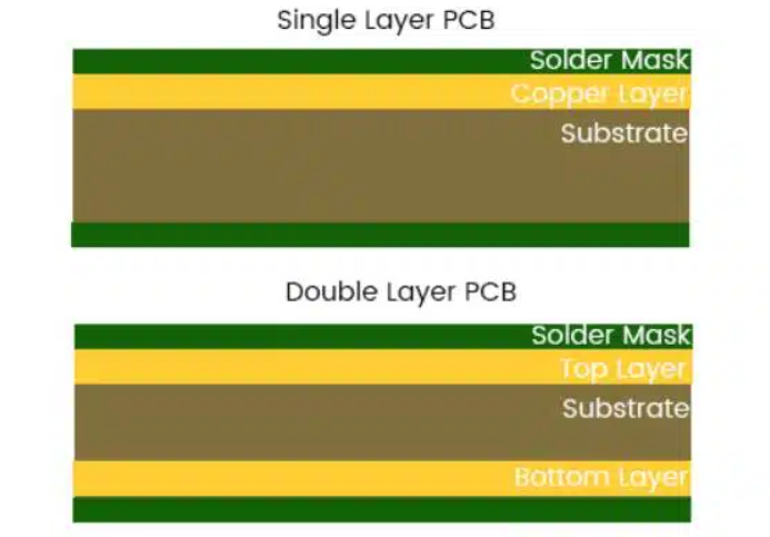
Single Layer versus Double Layer PCB
Single layer PCBs have one conductive layer, typically copper, on a non-conductive substrate. They are simple, cost-effective, and ideal for basic projects like hobbyist LED circuits. However, they limit routing options and component density due to space constraints.
Double layer PCBs feature conductive material on both sides of the substrate, connected through small holes called vias. This setup doubles the space for traces, allowing more complex designs with better signal integrity. For hobbyists, double layer boards suit projects with microcontrollers or multiple components, though they cost more to produce.
Choosing between single and double layer depends on project needs. Simple circuits benefit from single layer simplicity, while intricate designs require double layer flexibility.
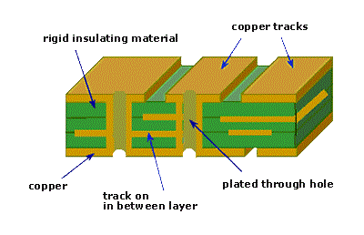
Multilayer PCBs and Their Role
Beyond double layer, multilayer PCBs stack multiple conductive layers separated by insulating material. Common in advanced electronics, they range from four to over ten layers. These boards handle high density circuits, reduce electromagnetic interference, and support compact designs. For hobbyists, multilayer PCB is less common due to cost and complexity, but they become relevant for sophisticated projects involving high speed signals. Understanding layer count helps in planning designs that balance functionality with budget constraints.
Core Materials in PCB Design
PCB materials play a critical role in performance and durability. The substrate, often made of fiberglass reinforced epoxy, provides structural support and insulation. Copper layers conduct electricity, forming the pathways for signals. A solder mask protects these layers from oxidation and short circuits, while silkscreen adds labels for component placement. Hobbyists should know that material choice affects thermal stability and electrical properties. Following industry standards ensures material reliability for various applications.
Traces and Vias in PCB Design
Traces and vias are fundamental to how signals travel across a PCB. Let's break down their purpose and importance for hobbyists venturing into PCB design.
What Are Traces?
Traces are thin lines of conductive material, usually copper, that connect components on a PCB. They act as wires, carrying electrical signals or power between points. Trace width and thickness determine current carrying capacity and resistance. Narrow traces suit low current signals, while wider ones handle higher power loads. For hobbyists, proper trace planning prevents overheating and signal loss. Industry guidelines, such as those from recognized standards, help in calculating safe trace dimensions for specific applications.
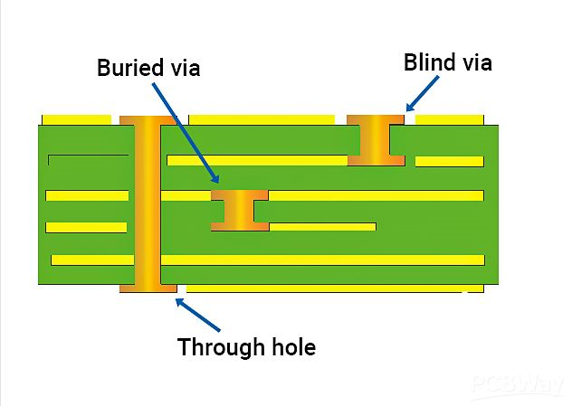
Understanding Vias
Vias are small holes in a PCB that connect different layers electrically. They allow traces to pass from one side of the board to another, essential in double layer and multilayer designs. Vias come in various types, including through hole, blind, and buried, each suited to specific routing needs. For hobbyists, through hole vias are the most common, as they are easier to implement in simpler designs. Correct via placement ensures signal integrity and avoids manufacturing issues.
Design Considerations for Traces and Vias
When designing traces and vias, spacing is crucial to prevent interference or short circuits. Traces should avoid sharp angles to minimize signal reflection, especially in high speed circuits. Vias must be placed strategically to reduce path length and maintain signal quality. Hobbyists should also consider the board's manufacturing limits, ensuring traces and vias meet minimum size requirements. Adhering to established design rules helps create functional and reliable PCBs for any project.
PCB Materials Tutorial for Hobbyists
Materials define a PCB's mechanical and electrical properties. For hobbyists, understanding these materials aids in selecting the right board for a project. The core substrate, often a composite of fiberglass and resin, offers strength and insulation. Copper layers, bonded to this substrate, form the conductive paths. Thickness of copper, measured in ounces per square foot, impacts current capacity. A protective solder mask layer prevents corrosion and accidental contact. Silkscreen, though not functional, assists in identifying component locations during assembly.
Material selection depends on application. Standard fiberglass substrates work for most hobbyist projects due to affordability and availability. For high frequency or high temperature environments, specialized materials may be needed, though they increase cost. Familiarity with material properties ensures designs withstand operational stresses while meeting performance goals. Following standards like those from recognized industry bodies guarantees material quality and compatibility.
Basic PCB Terminology Guide
- Substrate: The base material of a PCB, providing insulation and support.
- Copper Layer: Conductive material forming traces and pads for component connection.
- Solder Mask: Protective coating over copper to prevent shorts and oxidation.
- Silkscreen: Printed layer for labeling components and markings on the PCB.
- Via: A hole connecting different layers of a PCB electrically.
- Trace: Conductive path linking components on the board.
- Pad: Exposed copper area where components are soldered.
Understanding these terms simplifies communication with manufacturers and enhances design precision. As hobbyists progress, expanding this vocabulary will aid in tackling more complex projects and troubleshooting issues effectively.
Best Practices for PCB Design as a Hobbyist
Creating a functional PCB involves following proven design practices. Start with a clear schematic to map out component connections before layout. Place components logically, grouping related parts to minimize trace length. Keep power and ground traces short and direct to reduce noise. Ensure adequate spacing between traces to avoid interference, following minimum clearance rules from industry standards.
Use vias sparingly in multilayer designs to maintain signal integrity. Test designs virtually using simulation tools to identify potential flaws before manufacturing. Label components clearly on the silkscreen for easy assembly. Finally, review design rules specific to your fabrication process to prevent errors. These steps help hobbyists build reliable PCBs suited to their project goals.
Conclusion
Grasping PCB basics such as layers, traces, and vias equips electronic hobbyists with the foundation to create effective circuit designs. From understanding single layer versus double layer PCB options to mastering trace routing and via placement, each element plays a vital role in functionality. Familiarity with PCB materials and terminology further enhances design capability. By applying best practices, hobbyists can avoid common mistakes and build reliable projects. This knowledge not only boosts confidence but also opens doors to more complex electronic endeavors in the future.
FAQs
Q1: What are the main differences in single layer vs double layer PCB for beginners?
A1: Single layer PCBs have one conductive side, making them simple and affordable for basic projects like LED circuits. Double layer PCBs offer conductive layers on both sides, connected by vias, allowing more complex routing and higher component density. For hobbyists, single layer suits straightforward designs, while double layer supports advanced circuits with better space efficiency.
Q2: How do traces and vias in PCB design impact performance?
A2: Traces carry signals or power between components, and their width affects current capacity and resistance. Vias connect layers, enabling multilayer routing. Poor trace design can cause signal loss or overheating, while misplaced vias may disrupt signal integrity. Proper planning of both ensures reliable performance in hobbyist projects.
Q3: What should hobbyists know about PCB materials in this tutorial?
A3: Hobbyists should understand that PCB materials like fiberglass substrates provide insulation, while copper layers conduct electricity. Solder mask protects against shorts, and silkscreen aids assembly. Choosing standard materials keeps costs low for simple projects, but specific applications may require specialized options for heat or frequency demands.
Q4: Why is a basic PCB terminology guide useful for new designers?
A4: A basic PCB terminology guide helps new designers understand key concepts like substrate, traces, and vias. This knowledge simplifies design processes, improves communication with manufacturers, and reduces errors. For hobbyists, mastering these terms builds a strong foundation for tackling more intricate electronic projects over time.
References
IPC-6012E — Qualification and Performance Specification for Rigid Printed Boards. IPC, 2020.
IPC-A-600K — Acceptability of Printed Boards. IPC, 2020.


