Introduction
For electrical engineers, the design of a printed circuit board is a critical step in ensuring the functionality and reliability of electronic devices. A key aspect of this design process is understanding the PCB stackup, which defines the arrangement of layers in a multilayer board. This structure directly impacts signal integrity, electromagnetic compatibility, and thermal management. A well planned stackup can prevent issues like crosstalk and impedance mismatches, while a poorly designed one can lead to costly redesigns. This article explores the principles behind PCB stackup design, its importance in modern electronics, and best practices for creating effective solutions. By mastering these concepts, engineers can develop the best solution PCBs for high performance applications, ensuring both efficiency and durability in their designs.
What Is PCB Stackup and Why It Matters
A PCB stackup refers to the arrangement of conductive and insulating layers in a multilayer circuit board. These layers include signal layers for routing traces, power and ground planes for stable voltage distribution, and dielectric materials that separate them. The stackup configuration determines how electrical signals travel through the board and how well the design handles interference and power delivery.
The significance of a proper stackup cannot be overstated. It directly affects signal integrity by controlling impedance and minimizing noise. It also plays a vital role in managing electromagnetic interference, ensuring that high speed signals do not interfere with each other. Additionally, the stackup influences thermal dissipation, as the placement of planes and materials impacts heat distribution. For engineers working on complex designs, such as high speed digital circuits or power electronics, understanding PCB stackup is essential for achieving reliable performance and avoiding failures during operation.
Technical Principles of PCB Stackup Design
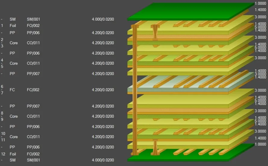
The design of a PCB stackup is governed by several engineering principles that ensure optimal electrical performance. First, the number of layers must be determined based on the complexity of the circuit. Simple designs may require only two layers, while advanced systems often need six, eight, or more. The choice depends on routing density, signal types, and power requirements.
Layer arrangement is another critical factor. Signal layers are typically placed adjacent to ground or power planes to provide a return path for currents and reduce noise. This proximity helps maintain controlled impedance, a key parameter for high speed signals. The dielectric material between layers also affects impedance and signal speed, as its thickness and permittivity influence electrical characteristics.
Symmetry in the stackup is important to prevent mechanical stress and warpage during manufacturing. An unbalanced design, where layers are unevenly distributed, can cause the board to bend under thermal or mechanical loads. Engineers must also consider via placement, as these connections between layers impact signal integrity and manufacturing complexity. Adhering to standards like IPC-6012E helps ensure that stackup designs meet performance and reliability criteria.
Best Practices for Designing PCB Stackups
Creating an effective PCB stackup requires careful planning and adherence to best practices tailored to the specific application. Below are actionable guidelines for engineers aiming to develop the best solution PCBs through optimal stackup design.
- Determine Layer Count Early: Assess the circuit requirements to decide on the number of layers. Consider factors like signal density and power distribution needs. More layers provide flexibility but increase cost and complexity.
- Prioritize Ground and Power Planes: Place ground and power planes close to signal layers to minimize loop inductance and ensure stable voltage. This setup also reduces electromagnetic interference.
- Maintain Symmetry: Arrange layers symmetrically around the board's center to avoid warpage. For instance, in an eight layer board, balance signal and plane layers on both halves.
- Control Impedance: Use dielectric materials with consistent thickness and properties to achieve target impedance for high speed signals. Reference standards like IPC-2141A for guidance on impedance calculations.
- Optimize Via Usage: Minimize the use of vias in high speed signal paths to reduce signal degradation. When necessary, use back drilling to remove unused via stubs.
Material selection is equally important. Choose dielectric materials with appropriate thermal and electrical properties to match the design needs. For high frequency applications, low loss materials are preferred to maintain signal integrity. Consulting standards such as IPC-4101E can provide specifications for selecting suitable laminates and prepregs.
Stackup Configurations for Different Applications
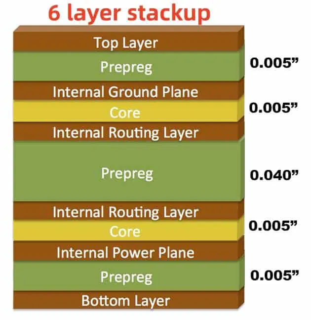
Different applications demand unique stackup configurations to address specific challenges. For high speed digital circuits, a common approach is to use a six layer PCB stackup with dedicated ground and power planes sandwiching signal layers. This setup ensures controlled impedance and reduces crosstalk between traces.
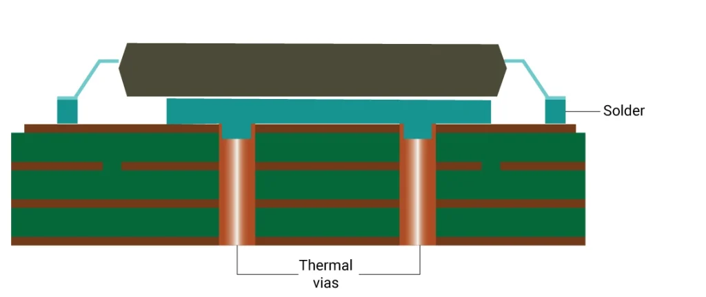
In power electronics, stackups often prioritize thick copper layers and thermal vias to handle high currents and dissipate heat. Ground planes are placed strategically to minimize voltage drops and improve stability. Standards like IPC-2152 provide guidelines for determining current carrying capacity based on trace width and layer thickness.
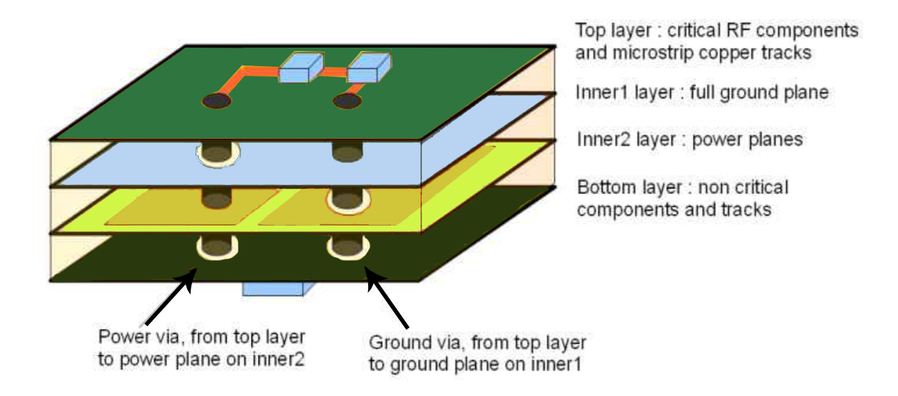
For radio frequency designs, microstrip and stripline configurations are used to manage signal propagation at high frequencies. These designs require precise dielectric spacing and ground plane placement to avoid signal loss. Engineers must also consider the stackup's impact on antenna performance if integrated into the board.
Common Challenges in PCB Stackup Design
Designing a PCB stackup is not without challenges. One frequent issue is impedance mismatch, which occurs when signal layers are not properly referenced to adjacent planes. This can lead to signal reflections and degraded performance. To mitigate this, engineers must calculate impedance based on layer spacing and material properties.
Another challenge is electromagnetic interference, especially in dense designs with mixed analog and digital signals. Separating sensitive signals and using shielding planes can help reduce interference. Crosstalk between adjacent traces is also a concern, particularly in high speed designs. Increasing spacing or adding ground traces between signals can address this issue.
Thermal management poses additional difficulties in power heavy applications. Poor layer arrangement can trap heat, leading to component failure. Incorporating thermal vias and balancing copper distribution across layers can improve heat dissipation. Adhering to standards like IPC-2221B ensures that thermal and mechanical aspects are considered during design.
Tools and Techniques for Stackup Planning
Modern PCB design tools allow engineers to simulate and validate stackup configurations before manufacturing. These tools calculate impedance, predict signal behavior, and identify potential interference issues. Layer stack editors within design software enable precise definition of layer thickness, material properties, and via structures.
Simulation is a valuable technique for optimizing stackup designs. It helps engineers test different configurations under virtual conditions, reducing the need for physical prototypes. Signal integrity analysis can reveal problems like crosstalk or reflections, while power integrity simulation ensures stable voltage distribution across planes.
Documentation is crucial for successful stackup implementation. Detailed stackup drawings and specifications should be prepared and shared with manufacturing teams to avoid miscommunication. Following guidelines from IPC-A-600K ensures that the final board meets acceptability criteria for layer alignment and material quality.
Conclusion
Understanding the PCB stackup is a fundamental skill for electrical engineers tasked with designing reliable and high performing printed circuit boards. By grasping the principles of layer arrangement, impedance control, and thermal management, engineers can create stackups that meet the demands of modern electronics. Best practices, such as prioritizing ground planes and maintaining symmetry, contribute to developing the best solution PCBs for various applications. With careful planning and adherence to industry standards, challenges like interference and thermal issues can be effectively managed. A well designed stackup not only ensures functionality but also enhances the durability and efficiency of the final product.
FAQs
Q1: What is the importance of understanding PCB stackup in design?
A1: Understanding PCB stackup is crucial for ensuring signal integrity, minimizing interference, and managing thermal performance. A proper stackup design reduces issues like crosstalk and impedance mismatch, which are critical for high speed circuits. It also impacts manufacturing reliability and board durability, making it a key consideration for electrical engineers working on complex projects.
Q2: How can engineers find the best solution PCBs through stackup design?
A2: Engineers can achieve the best solution PCBs by optimizing stackup for specific needs, such as high speed or power applications. This involves selecting the right layer count, placing ground planes strategically, and controlling impedance. Following industry standards and using simulation tools further ensures the design meets performance and reliability goals.
Q3: What standards guide PCB stackup design for signal integrity?
A3: Standards like IPC-6012E and IPC-2141A provide guidelines for PCB stackup design, focusing on performance and signal integrity. IPC-6012E covers qualification and performance specifications, while IPC-2141A offers detailed information on controlled impedance. These standards help engineers create reliable and consistent designs for various applications.
Q4: How does layer symmetry affect PCB stackup performance?
A4: Layer symmetry in a PCB stackup prevents mechanical stress and warpage during manufacturing and operation. An unbalanced stackup can lead to bending under thermal loads, affecting reliability. Symmetrical designs ensure uniform stress distribution, maintaining board flatness and ensuring consistent electrical performance over time.
References
IPC-6012E — Qualification and Performance Specification for Rigid Printed Boards. IPC, 2020.
IPC-2141A — Design Guide for High-Speed Controlled Impedance Circuit Boards. IPC, 2004.
IPC-4101E — Specification for Base Materials for Rigid and Multilayer Printed Boards. IPC, 2021.
IPC-2152 — Standard for Determining Current Carrying Capacity in Printed Board Design. IPC, 2009.
IPC-2221B — Generic Standard on Printed Board Design. IPC, 2012.
IPC-A-600K — Acceptability of Printed Boards. IPC, 2020.


