What Defines an Asymmetrical Stackup in PCB Design?
In the realm of Printed Circuit Board (PCB) design, a stackup refers to the precise arrangement of conductive copper layers and insulating dielectric materials within a multilayer board. Traditionally, many designs employ a symmetrical stackup, where the layer structure is mirrored around the board's central axis to achieve balance. An asymmetrical stackup, however, deviates from this conventional balance by featuring an uneven distribution of layers or varying material properties on either side of the board's core. This deliberate imbalance allows designers to address highly specific electrical or mechanical requirements that symmetrical designs cannot readily accommodate.
For instance, an asymmetrical configuration might strategically position a greater number of signal layers on one side of the board to optimize routing pathways for high-speed signals, or it could integrate different dielectric materials to achieve precise impedance control in critical circuit sections. While this design approach can introduce manufacturing challenges, such as potential board warping, it offers distinct advantages for advanced and specialized applications.
Why Opt for an Asymmetrical Stackup? Key Benefits for PCB Designers
Asymmetrical stackups are not the default choice for general PCB designs, yet they prove exceptionally advantageous in particular scenarios where standard symmetrical layouts fall short. Here are compelling reasons to consider this advanced design strategy:
Strategic Performance Enhancements
● Optimized Impedance Control: By precisely adjusting the thickness of dielectric layers and the properties of materials on one side of the PCB, designers can fine-tune characteristic impedance for high-speed signals. For example, a thinner dielectric prepreg on the outer layers can help achieve a target 50-ohm impedance for critical signal traces more effectively.
● Enhanced Crosstalk Reduction: The strategic placement of solid ground planes in closer proximity to high-speed signal layers on one side of the board can significantly minimize electromagnetic coupling and, consequently, crosstalk between adjacent traces, which is particularly beneficial in densely routed designs.
● Effective EMI Mitigation: Asymmetrical designs enable more effective placement of dedicated shielding layers or robust ground planes near sensitive components or radiating traces. This strategic layering can dramatically reduce unwanted electromagnetic interference (EMI) both radiated from and coupled into the PCB.
● Improved Space Efficiency: When a design demands a higher density of routing on one specific side (e.g., to accommodate numerous surface-mounted components), an asymmetrical stackup can provide the necessary additional signal layers without unduly increasing the overall thickness of the PCB.
While these benefits are highly attractive, implementing asymmetrical stackups demands meticulous planning and execution to prevent issues such as thermal imbalance during fabrication or other manufacturing defects.
Step-by-Step Guide: Designing an Asymmetrical Stackup for PCBs
Developing an asymmetrical stackup that delivers optimal electrical and mechanical performance requires a structured approach. Follow this practical guide to ensure your design successfully meets all project goals.
Step 1: Clearly Define Project Requirements
Begin by precisely identifying the specific electrical and mechanical needs of your project. Is your paramount concern impedance control for ultra-high-speed signals? Is the primary goal to significantly reduce crosstalk between closely packed traces? Or is robust EMI reduction the overarching objective? For example, a PCB destined for a 5G communication module might require extremely tightly controlled 50-ohm impedance for RF signal paths, which would necessitate very thin dielectric layers on the outer sections of the stackup.
Step 2: Configure the Optimal Layer Arrangement
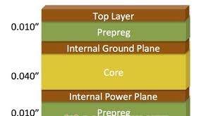
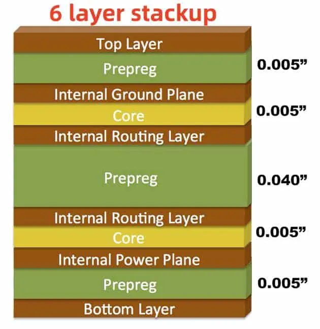
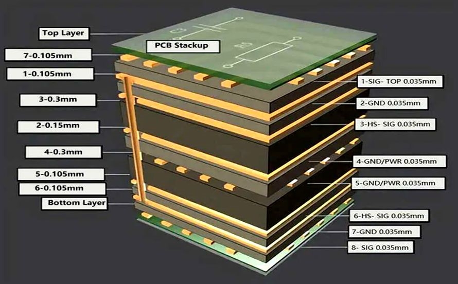
Unlike symmetrical stackups, where layers are evenly distributed and mirrored (e.g., a 4-layer board with two signal layers and two internal ground planes), an asymmetrical design might feature an unequal distribution, such as three signal layers on one side and a single power plane on the other. A typical 6 layer pcb stackup could be structured as follows:
● Layer 1: Signal (Top Layer)
● Layer 2: Ground Plane
● Layer 3: Signal
● Layer 4: Signal
● Layer 5: Power Plane
● Layer 6: Ground Plane (Bottom Layer)
This configuration prioritizes high-density signal routing on the upper portion of the board while ensuring continuous ground planes for effective shielding and return paths. It is highly recommended to use advanced simulation tools to validate the electrical performance of your proposed layer arrangement before finalizing the stackup.
Step 3: Meticulously Select Materials and Dielectric Thicknesses
Material selection is paramount in an asymmetrical stackup. Different dielectric thicknesses, or even entirely different material types (e.g., standard PCB FR4 material on one side and specialized high-frequency laminates on the other), can be utilized to achieve targeted electrical properties. For instance, employing a dielectric material with a lower dielectric constant (Dk) of 3.5 on the top layers can facilitate faster signal propagation compared to a material with a Dk of 4.2 on the bottom layers. Critical attention must be paid to potential differences in coefficients of thermal expansion (CTE) between mismatched materials, as significant disparities can lead to undesirable board warping during manufacturing.
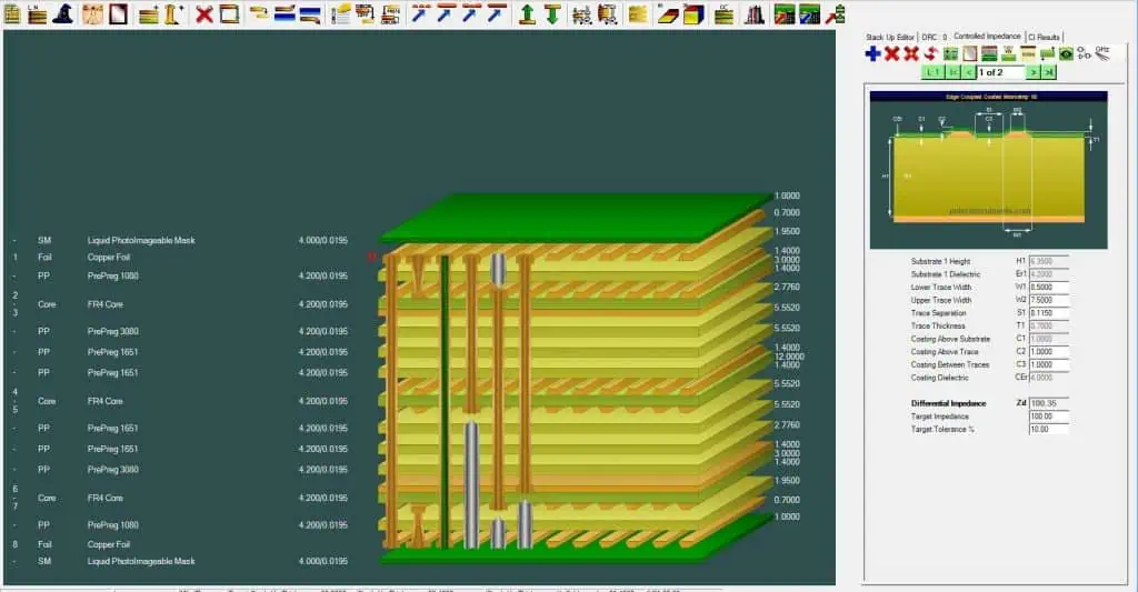
Step 4: Perform Comprehensive Impedance Simulations and Validation
Impedance mismatches are a leading cause of signal integrity degradation in high-speed designs. Utilize a 2D field solver or integrated PCB design software tools to accurately calculate the characteristic impedance of your signal traces. For a target single-ended impedance of 50 ohms, you might determine that a specific trace width (e.g., 6 mils) combined with a particular dielectric thickness (e.g., 4 mils) on the top layer is required. Adjust the stackup parameters if simulations reveal impedance deviations exceeding acceptable tolerances (e.g., typically ±10%).
Step 5: Address Potential Manufacturing Challenges Proactively
Asymmetrical stackups inherently carry a higher propensity for warping or bowing due to uneven stress distribution during the lamination process. Close collaboration with your PCB fabrication partner is essential to implement strategies that balance copper distribution and select core materials that minimize thermal mismatch. Some designers choose to incorporate non-functional or "dummy" copper fills on less dense layers to help even out thermal stresses, though this must be done judiciously to avoid impacting signal integrity.
Advanced PCB Design Tips for Asymmetrical Stackups
Beyond the foundational steps, incorporating these practical PCB design tips will ensure your asymmetrical stackup not only functions as intended but also excels in critical areas like impedance control, crosstalk reduction, and EMI mitigation.
1. Optimize Ground Plane Proximity for Crosstalk Control
Crosstalk, caused by unwanted electromagnetic coupling between adjacent traces, can significantly degrade signal quality. In an asymmetrical stackup, strategically place robust, continuous ground planes in close proximity to high-speed signal layers. For example, if layers 1 and 3 are dedicated high-frequency signal layers, ensure that layer 2 is a solid, uninterrupted ground plane. This configuration can reduce crosstalk by up to 30% in certain designs, based on typical industry simulations and best practices.
2. Leverage Differential Pairs for Superior Impedance Management
For all critical high-speed signals, it is best practice to route them as differential pairs. This technique inherently provides a more consistent characteristic impedance (e.g., 100 ohms for differential lines) and significantly enhances immunity to common-mode noise. Within an asymmetrical stackup, ensure that differential pairs are routed entirely on the same layer, and maintain precise trace length matching within the pair to prevent skew, which can introduce nanosecond-level timing errors.
3. Mitigate EMI Through Intelligent Layer Arrangement
Electromagnetic interference (EMI) can disrupt the functionality of nearby circuits and lead to failures in regulatory compliance testing. In an asymmetrical design, position sensitive analog signal layers as far as possible from inherently noisy digital or power delivery traces. Furthermore, placing a continuous ground plane directly beneath the top signal layer can serve as an effective electromagnetic shield, potentially reducing EMI radiation by as much as 20 dB across relevant frequency ranges, as evidenced by numerous design studies.
4. Maintain Copper Balance Where Possible
Even within an asymmetrical framework, strive to achieve a reasonable balance in copper distribution across all layers to minimize manufacturing-induced stresses. If one side of the board features particularly dense routing, consider adding non-functional copper pours or dummy fills on the opposite side to help distribute thermal mass more evenly. Unbalanced copper distribution can lead to board warpage or twist exceeding 0.5% of the board’s diagonal length, according to standard fabrication guidelines.
Addressing and Overcoming Common Asymmetrical Stackup Challenges
While asymmetrical stackups offer distinct advantages, they also present unique challenges. Here's how to effectively tackle the most common issues:
Thermal Imbalance and Warping
Challenge: Disparate layer counts or material types can lead to uneven thermal expansion and contraction during fabrication and operation, resulting in board warping.
Solution: Mitigate this by carefully selecting prepregs and core materials with closely matched coefficients of thermal expansion (CTE), ideally within 10-15 ppm/°C of each other. Work with your fabricator to ensure the lamination cycle is optimized for your specific material combination.
Signal Integrity Compromises
Challenge: Asymmetrical designs can complicate the creation of clear, low-impedance return paths for high-speed signals, potentially leading to increased delays and reflections.
Solution: Ensure continuous, uninterrupted ground planes are strategically placed directly adjacent to high-speed signal layers. These planes provide the necessary low-impedance return paths, crucial for preserving signal integrity. Avoid splitting ground planes beneath critical signals.
Elevated Manufacturing Costs
Challenge: Custom or highly specialized asymmetrical stackups often incur higher fabrication costs due to specialized materials and more complex processing requirements.
Solution: Optimize your design extensively early in the development cycle through detailed simulations to minimize the need for costly revisions. Maintain clear, comprehensive communication with your PCB manufacturer regarding all stackup specifications, material choices, and acceptable tolerances to manage expectations and costs effectively.
Essential Tools and Resources for Asymmetrical Stackup Design
Designing an effective asymmetrical stackup is significantly streamlined with the use of appropriate software tools. Many contemporary PCB design platforms now integrate sophisticated stackup editors and simulation capabilities to analyze impedance and signal integrity. When selecting software, look for features such as:
● Layer Stackup Builders: Visual tools that allow you to intuitively arrange and manage asymmetrical layer configurations.
● Integrated Impedance Calculators: Functionality to accurately predict trace characteristic impedance (e.g., for achieving 50 ohms for single-ended signals or 100 ohms for differential pairs).
● EMI and Crosstalk Analysis Modules: Advanced simulation capabilities to identify potential interference issues before physical fabrication.
Furthermore, fostering a collaborative relationship with your PCB fabrication partner is invaluable. Many manufacturers provide specialized stackup design guides or online calculators tailored to their specific processes, which can be crucial for ensuring manufacturability and optimizing performance.
Real-World Applications of Asymmetrical PCB Stackups
Asymmetrical stackups are particularly well-suited for a variety of specialized electronic fields where performance demands are stringent:
● RF and Microwave Systems: These applications frequently require exceptionally precise impedance control (e.g., exact 50-ohm characteristic impedance for RF transmission lines) and minimal EMI. Asymmetrical layering, often involving high-frequency dielectric materials on specific sides, can effectively achieve these goals.
● High-Speed Digital Interfaces: In complex applications such as DDR4/DDR5 memory interfaces or high-speed serial links, asymmetrical stackups are instrumental in managing signal density, controlling impedance, and mitigating crosstalk for data rates often exceeding 3.2 Gbps per pin.
● Mixed-Signal Systems: For boards integrating both sensitive analog and noisy digital circuitry, asymmetrical designs provide a powerful mechanism for physical and electrical separation, thereby reducing inter-domain interference and improving overall system performance.
Conclusion: Mastering Asymmetrical Stackups for Superior PCB Performance
An asymmetrical stackup represents a powerful and flexible tool for PCB designers who are tackling complex challenges such as precise impedance control, effective crosstalk reduction, and robust EMI mitigation. By meticulously planning your layer arrangement, judiciously selecting appropriate dielectric materials, and diligently adhering to established best practices, you can successfully leverage the inherent benefits of this unconventional approach without sacrificing manufacturability or overall performance. Utilize the detailed steps and advanced PCB design tips provided in this guide to confidently create boards that not only meet but exceed the stringent demands of modern electronics, from cutting-edge high-speed digital systems to highly sensitive RF applications.
By focusing on practical solutions and drawing upon real-world insights, this comprehensive guide equips you with the essential knowledge to confidently experiment with asymmetrical stackups. Start with smaller, less complex designs, perform extensive simulations at every stage, and maintain strong collaboration with your fabrication team to continuously refine your designs. The ultimate result will be a PCB that not only fulfills but significantly surpasses your project's performance requirements, standing as a testament to advanced design prowess.


