Introduction
In modern PCB designs, vias serve as critical interconnects between layers, enabling complex routing in multilayer boards. However, poor via design can introduce significant signal integrity challenges, especially at high frequencies where signals exceed gigabit per second rates. PCB via design signal integrity becomes paramount as data rates increase, leading to issues like reflections, crosstalk, and attenuation. Engineers must understand how vias disrupt controlled impedance transmission lines and contribute to overall system performance degradation. This article explores the effects of via inductance and capacitance, along with strategies for minimizing via effects to ensure reliable high-speed operation. By optimizing via configurations, designers can maintain signal quality across demanding applications.
Understanding Vias in PCB Design
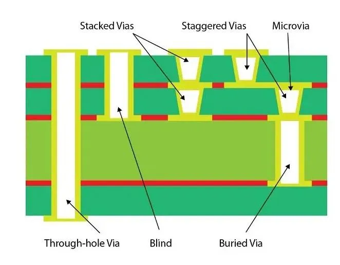
Vias are plated through-holes that provide vertical electrical connections in printed circuit boards. Common types include through-hole vias that span the entire board thickness, blind vias connecting surface to inner layers, and buried vias linking only inner layers. Microvias, with diameters typically under 150 microns, offer finer pitch and shorter lengths for high-density interconnects. Each type impacts signal propagation differently due to variations in length and parasitic elements. In high-speed designs, selecting the appropriate via type directly influences PCB via design signal integrity. Proper via selection aligns with layer stackup and routing constraints to avoid unnecessary discontinuities.
Engineers evaluate via types based on board thickness, layer count, and signal speed requirements. Through-hole vias, while cost-effective, introduce longer stubs that reflect signals in frequencies above several gigahertz. Blind and buried vias reduce stub lengths, improving performance in controlled impedance environments. Microvias excel in dense designs by minimizing inductance and enabling shorter signal paths. Compliance with IPC-2221 guidelines ensures via dimensions support reliable fabrication and electrical performance. Thoughtful via planning prevents routing congestion and maintains uniform signal characteristics.
Technical Principles of Via Parasitics
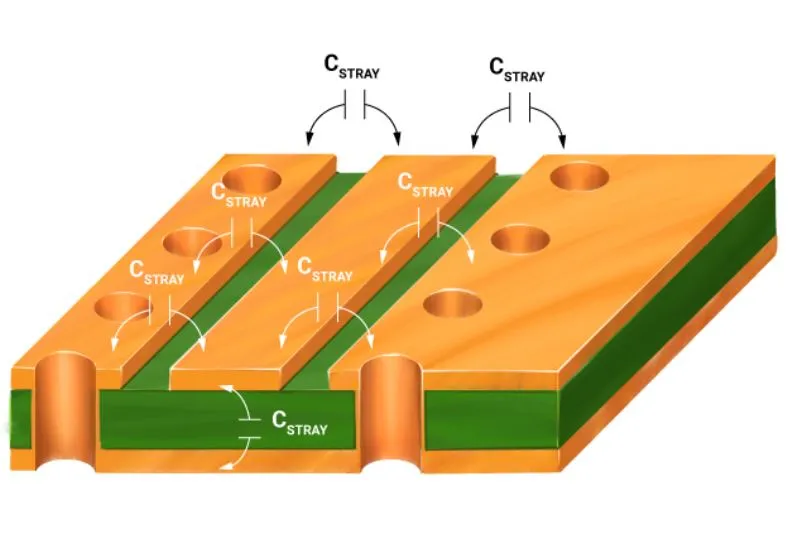
Via parasitics primarily consist of inductance and capacitance, which create impedance discontinuities in transmission lines. Via inductance arises from the magnetic field around the current-carrying conductor, scaling approximately with via length and inversely with diameter. Longer vias exhibit higher inductance, causing inductive reactance that slows rise times and increases overshoot in digital signals. This effect becomes pronounced when via length approaches a significant fraction of the signal wavelength. Via capacitance forms between the via barrel and nearby reference planes, influenced by antipad size and dielectric properties. Excessive capacitance leads to impedance drops, broadening pulses and degrading eye diagrams.
The interaction of via inductance and capacitance determines the via's characteristic impedance, often mismatched to the trace impedance of 50 or 100 ohms. At high frequencies, this mismatch generates reflections quantified by return loss. Crosstalk between adjacent vias further complicates signal integrity due to mutual inductance and capacitance coupling. Engineers model these parasitics using field solvers to predict insertion loss and near-end crosstalk. Understanding these principles guides via placement and geometry adjustments. Minimizing via effects requires balancing these parasitics against manufacturing capabilities.
Via inductance dominates in single-ended signals where return paths are distant, amplifying voltage swings during transitions. Capacitance effects intensify with closer plane proximity, altering signal delay and skew in differential pairs. Frequency-dependent skin effect increases effective via resistance, contributing to attenuation. Thermal expansion during operation can shift parasitics, necessitating robust designs. Standards like IPC-2221 provide baseline dimensions for pads and antipads to control these effects. Systematic analysis reveals how via geometry tunes impedance profiles for better matching.
Impacts of Poor Via Design on Signal Integrity
Suboptimal via design manifests as signal degradation across multiple metrics. Reflections from impedance steps cause ringing and overshoot, violating timing margins in high-speed interfaces. Increased via inductance slows edge rates, reducing eye opening and bit error rates in serial links. Via capacitance introduces low-pass filtering, attenuating high-frequency components essential for data integrity. In dense layouts, via-to-via coupling exacerbates crosstalk, injecting noise into adjacent signals. These combined effects limit maximum data rates and require additional margins in stackup planning.
At multi-gigabit speeds, via stubs act as resonators, generating resonances that corrupt harmonics. Power integrity suffers indirectly as via noise couples to power planes, creating ground bounce. Thermal vias for heat dissipation can inadvertently worsen signal vias if not isolated properly. Empirical measurements using time-domain reflectometry confirm these issues in prototypes. Addressing them early prevents costly respins. PCB via design signal integrity optimization thus integrates with overall board-level simulation.
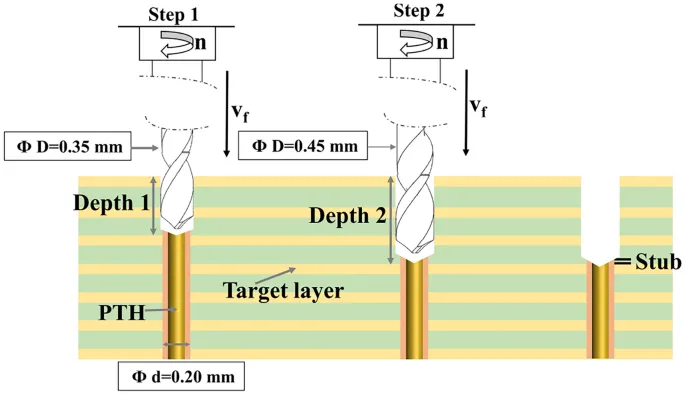
Long via stubs in through-hole configurations pose the greatest risk, reflecting up to 20-30% of incident energy at resonant frequencies. Microvias mitigate this by limiting stub lengths to fractions of wavelengths. Differential signals demand paired via optimization to preserve balance. Fabrication tolerances in plating thickness amplify inductance variations. Post-layout verification against simulation ensures predicted integrity holds. Proactive design rules preserve margins for process variations.
Optimization Strategies for Via Design
Effective strategies begin with minimizing via count on critical high-speed nets. Route signals on fewer layers using blind or buried vias to shorten transitions. Employ microvias for surface-layer connections, leveraging their low inductance for microvias signal integrity. Backdrilling removes unused stub lengths in through vias, tailoring effective height to signal needs. This technique reduces reflections while maintaining mechanical strength. Pair signal vias with adjacent ground vias for return current paths, forming shielded structures that lower inductance.
Antipad sizing critically controls capacitance; larger antipads reduce capacitive loading but increase stub resonance risks. Optimize pad stacks with tapered transitions to smooth impedance profiles. Controlled depth drilling for blind vias ensures precise stub removal. Stitching vias around high-current paths stabilize reference planes, minimizing via inductance impacts. These practices align with IPC-6012 performance specifications for multilayer boards. Iterative simulation refines geometries before fabrication.
For differential pairs, symmetric via placement preserves mode conversion immunity. Ground via fencing around clusters suppresses crosstalk. In HDI boards, stacked microvias enable any-layer interconnects with superior microvias signal integrity. Laser drilling achieves finer aspect ratios, supporting tighter pitches. Post-drill plating uniformity prevents resistance hotspots. Validation through vector network analyzer sweeps confirms optimization efficacy.
Advanced techniques include filled vias for thermal and mechanical reliability without compromising electrics. Elliptical or rectangular vias reduce inductance in space-constrained areas. Hybrid via farms combine types for mixed-signal boards. Layer sequencing prioritizes signal layers adjacent to planes for low-inductance returns. Fabrication partners provide design rule checks compliant with standards. These strategies holistically minimize via effects.
Practical Implementation and Troubleshooting
Designers implement via rules in constraint managers, enforcing minimum antipad clearances and drill sizes. Pre-layout planning allocates via budgets per net class. Post-route audits flag excessive vias or poor shielding. Simulation tools model 3D fields for accurate parasitics extraction. Prototype testing with eye pattern analysis verifies predictions. Common pitfalls include overlooking via resonance in harmonic analysis.
Troubleshooting distorted signals often traces to via stubs; backdrilling resolves many cases. Crosstalk spikes indicate insufficient ground via density; adding stitches cures it. Skew in pairs stems from asymmetric capacitances; symmetrizing fixes alignment. Thermal cycling exposes plating cracks increasing resistance; robust plating specs prevent recurrence. Documenting rules in design handoffs ensures consistency. These steps elevate PCB via design signal integrity across projects.
Conclusion
Via design profoundly influences PCB signal integrity through inductance, capacitance, and discontinuities. Strategic use of microvias, backdrilling, and shielding minimizes these effects, enabling higher data rates. Adhering to standards like IPC-2221 and IPC-6012 ensures manufacturable, reliable outcomes. Engineers benefit from modeling, simulation, and verification workflows. Implementing these optimizations sustains performance in evolving high-speed applications. Prioritizing via quality yields robust, future-proof boards.
FAQs
Q1: What role does via inductance play in PCB via design signal integrity?
A1: Via inductance arises from the via's length and diameter, creating inductive reactance that slows signal edges and causes overshoot at high frequencies. It disrupts controlled impedance, leading to reflections and reduced eye margins. Minimizing via length with blind or microvias lowers inductance. Ground vias nearby provide low-inductance return paths. Proper modeling predicts and mitigates these effects for reliable transmission.
Q2: How does via capacitance affect high-speed signals?
A2: Via capacitance between the barrel and planes causes impedance drops, broadening pulses and attenuating harmonics. Larger antipads reduce capacitance but risk stub resonances. Optimization involves balancing antipad size with plane proximity. In differential routing, symmetric capacitance preserves balance. This ensures minimal insertion loss and crosstalk in dense layouts.
Q3: What are effective ways of minimizing via effects in PCB design?
A3: Key methods include using shorter microvias or buried vias, backdrilling stubs, and adding shield vias. Reduce via count on fast nets and optimize antipads for impedance matching. Stitching grounds stabilizes planes. Simulation verifies parasitics before fabrication. These steps maintain signal quality per industry performance specs.
Q4: Why prioritize microvias signal integrity in HDI boards?
A4: Microvias offer short lengths and fine pitches, drastically cutting inductance and capacitance for superior high-frequency performance. They enable dense routing without long stubs. Laser processes achieve high aspect ratios reliably. In stackups, they support any-layer vias for shortest paths. This enhances eye diagrams and supports multi-gigabit rates effectively.
References
IPC-2221B — Generic Standard on Printed Board Design. IPC, 2003
IPC-6012E — Qualification and Performance Specification for Rigid Printed Boards. IPC, 2017
IPC-6012DS — Qualification and Performance Specification for Rigid Printed Boards with Embedded Components. IPC, 2020