Introduction
As electronic devices demand ever-higher integration levels, printed circuit board designers face the challenge of packing more functionality into smaller footprints. Via-in-pad technology emerges as a critical solution, enabling vias to be embedded directly within component pads rather than offset to the side. This technique is particularly vital for high-density interconnect (HDI) boards, fine-pitch ball grid arrays (BGAs), and applications requiring stringent signal and thermal management. By eliminating the need for additional routing traces around pads, via-in-pad maximizes available surface area for components and interconnects. Engineers must navigate specific via-in-pad design rules to ensure reliability, while addressing via-in-pad manufacturing challenges that can impact yield and performance. Ultimately, this approach balances density gains with practical fabrication constraints.
What Is Via-in-Pad and Why It Matters
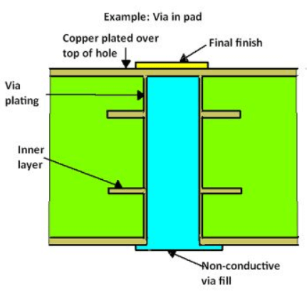
Via-in-pad refers to a PCB fabrication method where the via hole is drilled directly into the copper pad designated for component attachment, such as solder lands for BGAs or surface-mount devices. Unlike traditional dog-bone or staggered via configurations, the via shares the same land geometry, requiring subsequent filling and capping to create a planar surface compatible with soldering. Common implementations include non-conductive epoxy-filled vias tented with solder mask or conductively filled vias plated over for electrical continuity. This design choice becomes indispensable in multilayer HDI stacks where outer-layer routing density exceeds standard capabilities. Via-in-pad matters because it directly supports miniaturization trends in consumer electronics, automotive systems, and telecommunications, allowing escape routing for thousands of I/Os under a single package. Without it, designers would sacrifice either board size or layer count, compromising overall system performance.
The relevance extends to electrical engineers optimizing for high-speed signals and power delivery. In dense layouts, conventional vias consume precious real estate, forcing longer traces that introduce inductance and crosstalk. Via-in-pad mitigates these issues by providing the shortest possible interconnect path from component to inner layers. Furthermore, it facilitates microvia integration in HDI any-layer designs, adhering to evolving industry demands for sub-0.5 mm pitch components. As board complexity rises, mastering via-in-pad unlocks performance thresholds unattainable through legacy routing strategies.
Key Technical Principles of Via-in-Pad
The foundational principle of via-in-pad revolves around maintaining structural integrity during fabrication and assembly. The via must withstand drilling, plating, filling, and reflow without compromising the pad's solderability or annular ring. IPC-6012 establishes qualification criteria for rigid boards, specifying minimum annular ring dimensions to prevent breakout under thermal stress or drill wander. Designers calculate pad diameter as the finished hole size plus twice the required annular ring, plus fabrication tolerances for etch and plating. This ensures isolation between the via barrel and pad edge, critical for Class 2 or 3 products where reliability is paramount.
Plating uniformity represents another core mechanism, governed by aspect ratios typically limited to 1:1 or less for reliable copper deposition. High-aspect vias risk voids in electroless or electrolytic plating, leading to open circuits or electromigration failures over time. Filling materials, such as epoxy resins or conductive pastes, address planarity but introduce coefficient of thermal expansion (CTE) mismatches with copper. Proper cure cycles and post-fill lapping achieve flatness within microns, enabling uniform solder paste deposition. These principles collectively enable via-in-pad to support advanced stackups without sacrificing interlayer connectivity.
Signal propagation benefits from reduced via stubs, as the filled structure minimizes discontinuities in the transmission line. In high-frequency designs, stubs act as resonant elements, reflecting energy and degrading return loss. By placing the via terminus flush with the pad surface, engineers achieve near-ideal impedance control, especially when tented or capped per IPC-4761 via protection guidelines. Thermal conduction follows similar logic, with arrays of filled vias acting as heat pipes to spread dissipation across planes.
Via-in-Pad Design Rules for Optimal Performance
Adhering to via-in-pad design rules begins with pad geometry tailored to component pitch and via dimensions. The pad must encompass the drill diameter, plating buildup, and IPC-compliant annular ring to accommodate misalignment during lamination or assembly. For instance, external layers demand larger rings than internal buried vias due to higher exposure to handling stresses. Minimum via-to-via spacing follows external trace rules, preventing bridging during solder mask application or reflow. Engineers specify fill type—conductive for thermal vias, non-conductive for signal—in fabrication notes to guide process selection.
Aspect ratio control limits drill depth relative to diameter, ensuring void-free plating essential for HDI transitions. Blind or buried vias in via-in-pad configurations require precise laser drilling or sequential buildup, aligning with IPC-2221 design guidelines for generic printed boards. Solder mask expansion over the via tent prevents wicking during reflow, where molten solder could fill the barrel and starve the joint. Component-specific rules, such as BGA land patterns, integrate via-in-pad by centering the hole under the solder ball, optimizing fanout to inner layers. Validation through simulation verifies crosstalk and impedance before tape-out.
Layer stackup influences rules, with symmetric builds mitigating warpage from fill-induced stresses. High-layer-count boards pair via-in-pad with microvias for staggered transitions, distributing mechanical loads. Final design rules checklists confirm compliance, flagging violations like inadequate clearance to adjacent features.
Via-in-Pad Manufacturing Challenges and Mitigation
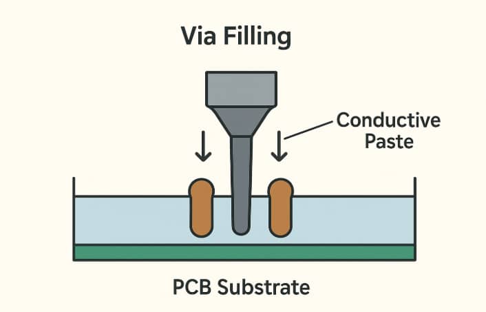
Fabrication introduces several via-in-pad manufacturing challenges, starting with via filling uniformity. Epoxy injection or screen-printed pastes must penetrate without air entrapment, followed by vacuum-assisted cure to expel volatiles. Shrinkage during polymerization can dimple the surface, necessitating chemical or mechanical planarization to restore coplanarity. Poor planarity leads to uneven solder paste volume, risking head-in-pillow defects or open joints in assembly.
Plating continuity poses risks if fill material interferes with barrel wall adhesion. IPC-4761 outlines protection schemes like Type VII (supported non-conductive fill with metal cap), mandating adhesion tests for long-term reliability. Solder mask registration over small features challenges exposure and development, potentially exposing via caps to contamination. Inspection via automated optical or x-ray verifies fill density and cap integrity, catching voids early.
Thermal cycling exacerbates CTE mismatches, potentially cracking the fill-copper interface. Sequential lamination for HDI mitigates this by building layers incrementally, allowing stress relief. Yield optimization hinges on fab capability matrices, rating processes like conductive fill for high-current paths.
Enhancing Signal Integrity with Via-in-Pad
Via-in-pad excels in via-in-pad signal integrity by eliminating stub lengths that plague dogleg vias. In high-speed SerDes or DDR interfaces, stubs couple extraneous modes, elevating insertion loss beyond 10 GHz. Filled vias present a smooth transition, maintaining characteristic impedance across the pad-via-plane junction. Back-drilling alternatives fall short in density-constrained areas, making via-in-pad preferable for 112 Gbps+ PAM4 links.
Crosstalk reduction follows from compact fanout, minimizing parallel trace lengths. Simulations reveal improved eye diagrams with via-in-pad, quantifying margin gains in timing and voltage. Ground via shielding around signal vias further suppresses far-end crosstalk, integral to dense routing channels.
Boosting Thermal Performance Through Via-in-Pad
Via-in-pad thermal performance leverages direct heat paths from component pads to inner copper planes. Arrays under power devices conduct via barrels, with conductive fills enhancing effective thermal conductivity beyond air-filled vias. Spreading angles from multiple vias distribute flux, lowering hotspot temperatures by coupling to heat sinks or embedded coins.
Finite element analysis guides array density, balancing thermal resistance with electrical parasitics. In power electronics, via-in-pad outperforms peripheral arrays by minimizing lateral gradients. Reliability improves as even dissipation reduces electromigration in traces.
Cost Considerations for Via-in-Pad Implementation
The cost of via-in-pad stems from specialized processes absent in standard through-hole boards. Filling, plating over fill, and planarization add steps, elevating per-panel expenses in HDI production. Conductive fills command premiums over non-conductive due to material and cure complexity. Inspection ramps up with x-ray for voids, impacting throughput.
Volume mitigates costs, as setup amortizes over panels, but prototypes incur high non-recurring engineering. Designers weigh trade-offs: density savings reduce layer count, offsetting fill premiums in mid-volume runs. Fab quotes factor via count, fill type, and class, guiding make-or-buy decisions.
Best Practices for Via-in-Pad Success
Select fill based on function: non-conductive for signals, conductive for thermals. Specify cap thickness and tenting in notes, aligning with J-STD-001 soldering requirements. Simulate early for SI and thermal, iterating pad sizes. Partner with fabs verifying IPC Class 3 annular rings. Prototype validates planarity via profilometry.
Conclusion
Via-in-pad technology transforms advanced PCB designs by maximizing density without forfeiting signal integrity or thermal performance. Engineers adept at via-in-pad design rules and aware of manufacturing challenges unlock HDI potential for next-generation systems. While the cost of via-in-pad demands justification through performance gains, best practices ensure reliable outcomes. As densities escalate, this technique remains a cornerstone for innovation.
FAQs
Q1: What are the primary via-in-pad design rules for high-reliability PCBs?
A1: Via-in-pad design rules emphasize annular ring per IPC-6012, pad sizing for drill plus tolerances, and via-to-pad clearances. Aspect ratios stay below 1:1 for plating, with solder mask expansion preventing wicking. Stackup symmetry aids warpage control. These rules support Class 3 qualification.
Q2: How do via-in-pad manufacturing challenges affect PCB yield?
A2: Challenges like fill voids, shrinkage dimples, and cap adhesion reduce yield if unmanaged. Vacuum filling and post-lap inspection per IPC-4761 mitigate risks. Sequential HDI buildup distributes stresses. Yield recovers with process tuning.
Q3: Why is via-in-pad signal integrity superior in high-speed designs?
A3: Via-in-pad eliminates stubs, preserving impedance and minimizing reflections. Shorter paths cut inductance, improving eye quality. Ground shielding enhances isolation. Simulations confirm gains over traditional fanout.
Q4: What impacts the cost of via-in-pad in production?
A4: Costs rise from filling, planarization, and inspection steps. Conductive fills and high via counts amplify expenses. Layer reductions offset in volume. Quotes balance complexity against density benefits.
References
IPC-6012E — Qualification and Performance Specification for Rigid Printed Boards. IPC, 2017
IPC-4761 — Via Protection Schemes and Fabrication Impact. IPC, 2020
IPC-2221 — Generic Standard on Printed Board Design. IPC, 2017
J-STD-001 — Requirements for Soldered Electrical and Electronic Assemblies. IPC/JEDEC, 2017


