Introduction
In the realm of printed circuit board (PCB) design, the integration of advanced techniques is vital for optimizing space and performance, especially with ball grid array (BGA) components. One such technique, via-in-pad, involves placing vias directly within the pads of surface mount components, often used in fine pitch BGAs to address routing challenges. When implemented without a traditional PCB fanout strategy, this approach can significantly alter design outcomes. This article explores the advantages and disadvantages of using via-in-pad without fanout, focusing on its implications for BGA layouts, land and via configurations, and overall board performance. Aimed at electrical engineers, the discussion provides a detailed look into how this method impacts design efficiency and manufacturing reliability while adhering to industry standards for high-density interconnects.
What Is Via-in-Pad Without Fanout and Why It Matters
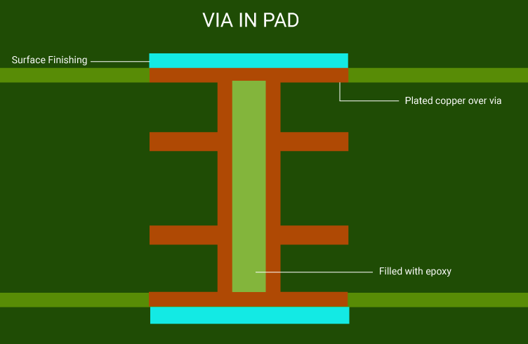
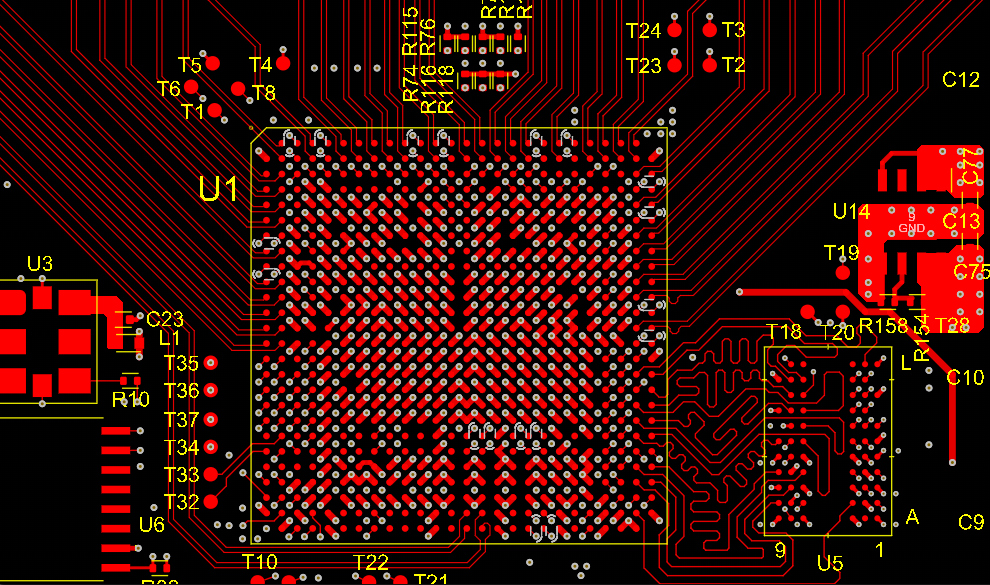
Via-in-pad is a design technique where vias are placed directly under the pads of components, such as BGAs, rather than in separate areas of the fast turn PCB. This is particularly useful for fine pitch BGAs, where the spacing between pads is minimal, making traditional routing difficult. Normally, PCB fanout refers to the process of routing traces from BGA pads to vias located outside the component footprint, allowing for easier connections to other layers. However, when via-in-pad is used without fanout, the vias are positioned directly within the pad, eliminating the need for additional trace routing on the surface layer.
This approach matters because it addresses the growing demand for miniaturization in electronics. With devices becoming smaller and more complex, maximizing PCB space is critical. Fine pitch BGAs, often with pad pitches below 0.5 mm, require innovative solutions to manage routing density. Via-in-pad without fanout can reduce the board’s footprint, but it also introduces unique challenges in design and manufacturing. Understanding its impact is essential for engineers working on high-density layouts where land and via placement directly influences signal integrity and thermal performance.
Technical Principles of Via-in-Pad Without Fanout
The principle behind via-in-pad without fanout lies in its ability to simplify routing for BGA components by embedding vias directly into the land areas. In a standard PCB fanout design, traces extend from BGA pads to nearby vias, which then connect to internal layers. This requires additional surface space and can complicate layouts for fine pitch BGAs. By contrast, via-in-pad places the via within the pad itself, often filled or plated over to maintain a flat surface for soldering.
From a technical perspective, this method reduces the trace length between the pad and via, minimizing parasitic inductance and capacitance. It is particularly beneficial for high-speed signals where signal integrity is a priority. However, the absence of fanout means that all connections rely on the via structure beneath the pad, which can strain manufacturing processes. The design must account for via filling techniques, as per standards like IPC-6012E, to prevent voids or defects during PCBA assembly. Additionally, the land and via configuration must ensure proper solder joint formation, as misalignment or poor filling can lead to reliability issues.
The approach also affects thermal dissipation. Vias directly under pads can act as thermal conduits, transferring heat away from components. Yet, without fanout, the surface area for heat spreading is limited, potentially leading to localized hotspots. Engineers must balance these factors when designing for high-power BGA applications, ensuring compliance with thermal management guidelines in standards such as IPC-A-600K.
Advantages of Via-in-Pad Without Fanout
Implementing via-in-pad without fanout offers several benefits, particularly for high-density PCB designs involving fine pitch BGAs. Below are the key advantages:
- Space Optimization: By eliminating the need for external fanout traces, this method frees up surface area on the PCB. It allows for tighter component placement, which is critical in compact designs where every square millimeter counts.
- Improved Signal Integrity: The direct connection between the pad and via reduces trace length, lowering the risk of signal degradation. This is especially valuable for high-speed applications where BGA components handle gigabit data rates.
- Enhanced Thermal Pathways: Vias under pads can provide a direct route for heat dissipation into inner layers or to a ground plane. When designed correctly, this can help manage thermal loads in dense layouts.
- Simplified Routing: Without fanout, the top layer routing complexity decreases, enabling designers to focus on internal layer connections. This can streamline the design process for fine pitch BGAs with numerous pins.
These advantages make via-in-pad without fanout a compelling choice for modern electronics, especially in applications like mobile devices and high-performance computing where space and performance are paramount. However, adherence to manufacturing standards, such as IPC-6012E for via filling, is crucial to realizing these benefits without compromising reliability.
Disadvantages of Via-in-Pad Without Fanout
Despite its benefits, via-in-pad without fanout presents notable challenges that engineers must consider during PCB design. The following points highlight the primary disadvantages:
- Manufacturing Complexity: Placing vias directly in pads requires advanced fabrication techniques, such as via filling or plating over, to ensure a smooth surface for soldering. Non-compliance with standards like IPC-A-600K can result in defects like solder voids or uneven pads.
- Increased Costs: The specialized processes needed for via-in-pad, such as filling with conductive or non-conductive materials, often raise production costs. This can be a significant drawback for budget-constrained projects.
- Limited Heat Spreading: Without fanout traces, the surface area for dissipating heat is reduced. This can lead to thermal concentration around BGA pads, posing risks for components sensitive to high temperatures.
- Assembly Challenges: The absence of fanout can complicate inspection and rework. Solder joint issues under the pad are harder to detect and repair, potentially affecting long-term reliability.
- Design Constraints: This approach may not suit all BGA configurations, especially those requiring extensive power and ground connections. Engineers might face difficulties in routing critical signals without sufficient surface traces.
These drawbacks underscore the importance of thorough planning and simulation during the design phase. Engineers must weigh these challenges against the space-saving benefits, ensuring that manufacturing capabilities align with design intent as per industry guidelines like IPC-6012E.
Practical Solutions and Best Practices
To mitigate the challenges of via-in-pad without fanout while leveraging its advantages, engineers can adopt several best practices. These solutions focus on design optimization and manufacturing readiness for BGA and fine pitch layouts.
- Adhere to Via Filling Standards: Ensure that vias in pads are filled or plated according to IPC-6012E guidelines. This prevents solder wicking and ensures a flat surface for component attachment.
- Optimize Land and Via Dimensions: Carefully design the land and via sizes to balance thermal and electrical performance. Standards like IPC-A-600K provide criteria for acceptable pad and via structures to avoid assembly issues.
- Use Thermal Vias Strategically: Incorporate additional thermal vias near high-power BGA components to enhance heat dissipation. Place them in areas that do not interfere with signal routing.
- Simulate Signal Integrity: Before finalizing the design, use simulation tools to verify signal integrity, especially for high-speed fine pitch BGAs. This helps identify potential issues caused by short trace lengths or via placement.
- Collaborate with Fabricators Early: Engage with manufacturing teams during the design stage to confirm process capabilities for via-in-pad without fanout. This reduces the risk of costly redesigns due to fabrication limitations.
By following these practices, engineers can achieve reliable PCB layouts that maximize the benefits of via-in-pad while minimizing risks. Documentation and adherence to standards are key to ensuring consistent outcomes in production.
Troubleshooting Common Issues
When working with via-in-pad without fanout, certain issues may arise during design or manufacturing. Addressing these proactively can save time and resources. For instance, solder joint defects often occur if vias are not properly filled, leading to uneven surfaces. Inspecting boards post-assembly using techniques outlined in IPC-A-600K can help identify such problems early. Another common concern is thermal imbalance, where heat accumulates around BGA pads. Adding supplementary vias or adjusting layer stackup for better heat distribution can resolve this.
Signal interference is also a potential issue, particularly with fine pitch BGAs handling high-speed data. If simulations indicate crosstalk or impedance mismatches, adjusting via placement or adding ground planes may be necessary. Finally, if manufacturing feedback highlights challenges with via filling, revisiting the design to include fanout for critical connections might be a practical compromise. These troubleshooting steps ensure that the design remains robust across various applications.
Conclusion
Via-in-pad without fanout presents a compelling solution for optimizing PCB space and enhancing signal integrity in BGA and fine pitch layouts. Its ability to reduce routing complexity and improve thermal pathways makes it ideal for high-density designs. However, the approach comes with trade-offs, including increased manufacturing costs, assembly challenges, and potential thermal issues. By adhering to industry standards like IPC-6012E and IPC-A-600K, engineers can navigate these challenges effectively. Careful design, simulation, and collaboration with fabrication teams are essential to achieving reliable outcomes. Ultimately, understanding the advantages and disadvantages of this technique allows for informed decisions in PCB design, ensuring performance and manufacturability align with project goals.
FAQs
Q1: What are the main benefits of using via-in-pad without fanout for BGA components?
A1: For BGA components, via-in-pad without fanout optimizes PCB space by eliminating external traces, allowing tighter layouts. It also enhances signal integrity by reducing trace lengths, which is crucial for high-speed applications. Additionally, it can improve thermal dissipation through direct via paths, provided designs follow standards like IPC-6012E for proper via filling.
Q2: How does via-in-pad without fanout impact PCB fanout strategies for fine pitch BGAs?
A2: Via-in-pad without fanout removes the need for traditional PCB fanout strategies by placing vias directly in pads of fine pitch BGAs. This simplifies top-layer routing but limits surface trace options, requiring careful planning for power and ground connections to avoid design constraints or signal issues.
Q3: What challenges arise with land and via configurations in via-in-pad designs?
A3: Land and via configurations in via-in-pad designs face challenges like manufacturing complexity and solder joint reliability. Improper via filling can lead to voids, while limited surface area affects heat spreading. Following IPC-A-600K guidelines for pad and via quality helps mitigate these risks during production.
Q4: How can engineers ensure reliability when using via-in-pad without fanout for PCB layouts?
A4: Engineers can ensure reliability by adhering to standards like IPC-6012E for via filling and using simulation tools to verify signal integrity. Early collaboration with fabricators, strategic thermal via placement, and thorough post-assembly inspection per IPC-A-600K are also critical for consistent performance in PCB layouts.
References
IPC-6012E — Qualification and Performance Specification for Rigid Printed Boards. IPC, 2020.
IPC-A-600K — Acceptability of Printed Boards. IPC, 2020.


