Introduction
In high-speed PCB designs, maintaining robust grounding and effective shielding stands as a cornerstone for achieving signal integrity and electromagnetic compatibility. Via stitching techniques address these challenges by interconnecting multiple layers through arrays of vias, particularly for ground planes. Electrical engineers often encounter issues like EMI radiation from plane discontinuities or high return path inductance, where via stitching provides a reliable solution. This comprehensive guide delves into via stitching for EMI reduction, via stitching spacing guidelines, grounding via placement strategies, and PCB shielding methods. By understanding these principles, designers can optimize multilayer boards for performance in demanding applications. The following sections outline the fundamentals, mechanisms, and best practices to implement via stitching effectively.
What Is Via Stitching and Why It Matters
Via stitching refers to the strategic placement of multiple vias in a pattern to electrically connect copper planes, typically ground planes, across different layers of a multilayer PCB. These vias form a distributed low-impedance path that mimics a solid plane connection, even over splits or cuts in the planes. Unlike a single via, which carries limited current and offers higher inductance, stitching uses redundancy to handle higher currents and frequencies. This technique proves essential in modern electronics where operating frequencies exceed hundreds of megahertz, and board densities increase.
The relevance of via stitching intensifies in environments demanding EMI compliance and thermal management. Poor grounding leads to elevated loop inductance, causing voltage drops and radiated emissions that fail regulatory tests. Via stitching mitigates these by providing multiple parallel paths, reducing overall inductance by factors proportional to the number of vias. For shielding, it creates barriers that confine electromagnetic fields, protecting sensitive circuits. In high-power or RF designs, it also aids heat dissipation by linking planes to thermal vias. Ultimately, incorporating via stitching enhances board reliability and performance margins.
Technical Principles Behind Via Stitching
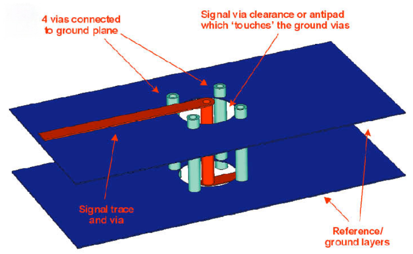
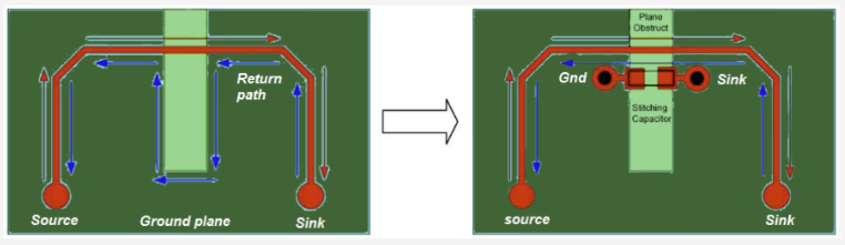
At its core, via stitching lowers the inductance of inter-layer connections, a critical factor in high-frequency signal propagation. Each via introduces some inductance, approximately 1 nH per mm of length, but arrays distribute this across parallel paths, yielding an equivalent inductance reduction. When a signal trace crosses a plane split, the return current seeks the lowest impedance path; without stitching, it detours around the split, enlarging the loop area and boosting magnetic field radiation. Stitching vias maintain continuity, confining the return path and minimizing loop area.
For EMI reduction, via stitching prevents plane edges or gaps from acting as slot antennas. Electromagnetic theory dictates that structures smaller than one-twentieth of the wavelength at the highest frequency avoid resonance. Thus, via stitching spacing guidelines follow this principle, with via centers spaced less than λ/20, where λ equals the wavelength c/f, c being the speed of light, and f the frequency. This dense placement forms a virtual continuous plane, suppressing far-field radiation. In shielding applications, rows of grounded stitching vias along perimeters or around components emulate a Faraday cage within the board stackup.
Grounding via placement further leverages skin effect at high frequencies, where currents flow on plane surfaces. Stitching ensures equipotential across layers, averting ground bounce. Per IPC-2221B guidelines for printed board design, such interconnections support controlled impedance and minimize crosstalk. These mechanisms collectively elevate PCB performance under dynamic electrical stresses.
Practical Solutions and Best Practices for Via Stitching
Implementing via stitching begins with identifying critical areas like plane splits, high-current paths, and sensitive analog sections. Place stitching vias along the edges of splits, spaced according to the board's maximum operating frequency. For via stitching spacing guidelines, calculate the wavelength for the highest harmonic, then set spacing to λ/20 or tighter for conservative designs; this ensures effective EMI suppression up to multi-GHz ranges. Use through-hole vias for simplicity in most cases, though blind or buried vias suit high-density boards to preserve surface area.
Grounding via placement demands symmetry and density around components. Surround IC ground pads with a fence of 4 to 8 vias within 1 mm, connecting to the nearest plane. For power distribution, apply similar stitching between power and ground planes to balance currents. PCB shielding methods incorporate perimeter stitching along board edges, forming a grounded enclosure that reflects external fields. Combine with guard traces between stitching rows for enhanced isolation in mixed-signal layouts.
Via stitching techniques vary by application: grid patterns for broad plane coverage offer isotropic paths, while linear fences suit trace shielding. Automate placement in design tools using pattern generators, verifying density with field solvers for EMI hotspots. Avoid clustering vias near drill exits to prevent breakout during fabrication, adhering to IPC-6012E specifications for rigid board performance. Thermal considerations include teardrop entries to reduce stress concentrations under reflow.
In high-speed designs, pair stitching with decoupling capacitors placed between vias for stitching capacitor effects, shunting high-frequency noise. Test prototypes with near-field probes to validate EMI reduction post-fabrication. These practices yield robust designs compliant with electromagnetic standards.
Common Mistakes and Troubleshooting in Via Stitching
Designers frequently overlook via density, spacing vias too far apart, which allows EMI leakage through effective slots. Compute spacing rigorously based on frequency; for a 1 GHz signal, λ/20 equates to about 15 mm in free space, adjusted for dielectric constants. Insufficient vias around splits cause return path deviations, manifesting as eye diagram closure or increased jitter. Simulate loop inductance pre-layout to quantify improvements.
Another pitfall involves asymmetric placement, creating ground potential gradients that couple noise into signals. Ensure even distribution, especially in asymmetric stackups. Fabrication issues arise from undersized vias unable to handle currents, leading to electromigration; select diameters compatible with aspect ratios per J-STD guidelines. During troubleshooting, review S-parameters for resonance peaks indicating poor stitching.
Over-stitching consumes drill cycles and increases cost without proportional benefits beyond λ/20 density. Balance via count with board constraints. Post-assembly EMI scans pinpoint deficiencies, allowing targeted additions in revisions. Logical verification against design rules prevents these errors.
Conclusion
Via stitching stands as an indispensable technique for electrical engineers tackling grounding and shielding in complex PCBs. By reducing inductance, enforcing return path integrity, and forming electromagnetic barriers, it excels in via stitching for EMI reduction and PCB shielding methods. Adhering to via stitching spacing guidelines and strategic grounding via placement ensures optimal performance across frequencies. Integrating these practices early in the design flow minimizes iterations and enhances reliability. As board speeds rise, mastering via stitching techniques will remain key to successful implementations.
FAQs
Q1: What are effective via stitching techniques for EMI reduction?
A1: Via stitching techniques for EMI reduction involve placing arrays of grounded vias along plane splits and high-speed trace vicinities. Dense patterns, spaced at λ/20 intervals, prevent slot resonances and confine fields. Combine with ground pours for comprehensive suppression. This approach maintains signal integrity in multilayer boards while complying with electromagnetic requirements.
Q2: How do via stitching spacing guidelines impact PCB performance?
A2: Via stitching spacing guidelines recommend intervals less than one-twentieth of the wavelength at peak frequencies to avoid antenna effects. Tighter spacing lowers inductance and bolsters shielding efficacy. Engineers calculate based on board harmonics, adjusting for dielectrics. Proper adherence reduces radiated emissions significantly.
Q3: What is the best grounding via placement strategy in multilayer PCBs?
A3: Optimal grounding via placement surrounds critical nets and plane discontinuities with redundant vias forming low-impedance paths. Position near component grounds and trace transitions for return current continuity. Symmetry prevents imbalances. This strategy aligns with design standards for robust performance.
Q4: How does via stitching contribute to PCB shielding methods?
A4: Via stitching enhances PCB shielding methods by creating grounded via fences that emulate Faraday cages internally. Rows along perimeters or enclosures block external interference and contain internal emissions. Integrated with plane layers, it provides multi-layer isolation. This proves vital for mixed-signal and RF applications.
References
IPC-2221B — Generic Standard on Printed Board Design. IPC, 2012
IPC-6012E — Qualification and Performance Specification for Rigid Printed Boards. IPC, 2015
J-STD-001H — Requirements for Soldered Electrical and Electronic Assemblies. IPC, 2018


