Introduction
If you are an electronic hobbyist building your first custom circuit board, you quickly discover that PCB traces form the essential pathways connecting all your components. These thin copper lines carry power and signals across the board, making your project functional. Understanding what PCB traces are sets the foundation for reliable PCB design, whether you are prototyping a simple LED blinker or a more complex microcontroller setup. This article serves as a complete PCB trace guide, explaining PCB traces in PCB design with practical insights tailored for hobbyists. You will learn what do PCB traces do, how to route them effectively, and tips to avoid common pitfalls. By the end, you will feel confident tackling your next PCB design traces project.
What Are PCB Traces?
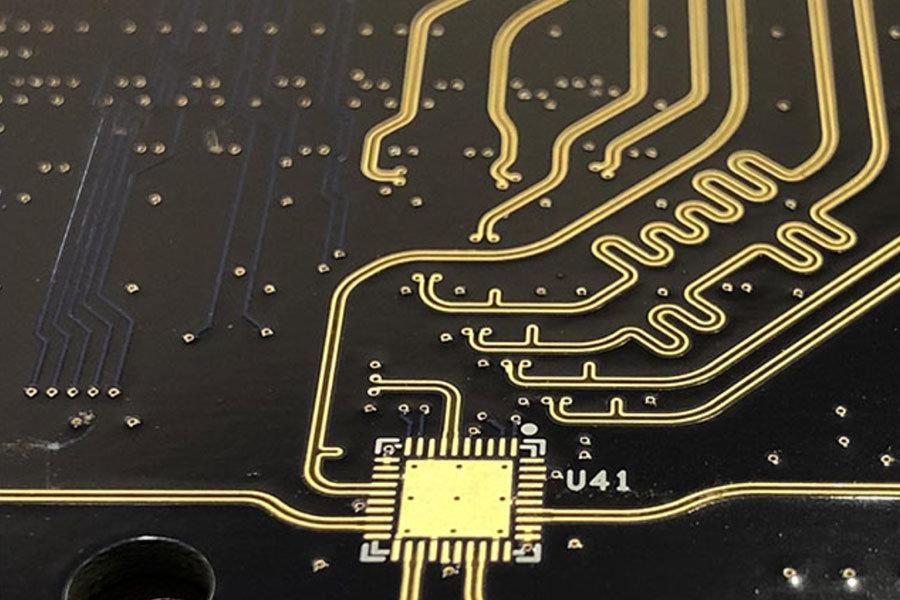
PCB traces are the conductive copper paths etched onto the surface layers or embedded within the internal layers of a printed circuit board. They replace traditional point-to-point wiring, providing a compact and organized way to interconnect electronic components like resistors, capacitors, and microcontrollers. In essence, PCB traces function as the roads on your circuit board, directing electrical current from one point to another. Without properly designed traces, signals can weaken, power delivery fails, or the entire board malfunctions. For hobbyists, grasping this basic definition of what are PCB traces helps when transitioning from breadboards to custom PCBs. These traces come in various shapes and sizes, adapted to handle different types of signals or power loads.
The manufacturing process starts with a copper-clad laminate, where unwanted copper is removed through etching to leave behind the desired trace patterns. This creates flat, narrow strips that adhere tightly to the board's insulating substrate, usually fiberglass-reinforced epoxy. Traces can span single-layer boards for simple hobby projects or multilayer stacks for advanced designs. Their placement follows the schematic, ensuring every connection matches the intended circuit logic. Hobbyists often begin with double-sided boards, using traces on both top and bottom layers connected via plated through-holes.
Why PCB Traces Matter in Electronic Hobby Projects
In PCB design traces play a pivotal role because they directly impact the performance, reliability, and manufacturability of your board. Poorly designed traces lead to issues like overheating, signal distortion, or intermittent failures, which can frustrate hobbyists during testing. Conversely, well-planned traces ensure clean power distribution and fast signal transmission, making your Arduino shield or sensor board work flawlessly. For electronic hobbyists, mastering PCB traces in PCB design means fewer prototypes and quicker successes in projects like robotics or IoT devices. Traces also influence the overall size and cost of your PCB, as wider or longer paths require more board space. Ultimately, they bridge the gap between your circuit idea and a working prototype.
Consider how traces handle everyday hobby tasks, such as powering motors or transmitting data from sensors. In high-speed projects, traces must minimize interference to preserve signal integrity. Even in low-speed designs, adequate trace sizing prevents voltage drops that dim LEDs or slow motors. This relevance underscores why every hobbyist needs a solid PCB trace guide. Ignoring trace fundamentals turns exciting builds into troubleshooting marathons.
Key Properties of PCB Traces
Several properties define how effectively PCB traces perform in a circuit. Trace width determines the amount of current it can carry without excessive heating, wider traces support higher loads like those for power rails. Thickness, often specified by copper weight in ounces per square foot, affects resistance and thermal dissipation, with standard thicknesses suiting most hobby applications. Length influences signal delay and potential crosstalk, so shorter paths are preferable for time-sensitive signals. Material purity and surface finish also play roles in conductivity and solderability. These factors interlink, requiring balanced choices during PCB design traces.
Routing geometry adds another layer, as straight lines reduce resistance compared to meandering paths. Sharp corners can create weak points prone to cracking under thermal stress. Spacing between adjacent traces prevents electrical shorts and electromagnetic interference. Vias, small plated holes, allow traces to jump layers, essential for dense layouts. Hobbyists benefit from understanding these properties to optimize simple boards without overcomplicating designs.
Standards like IPC-2221 provide guidelines for selecting trace dimensions based on electrical requirements, ensuring designs meet basic reliability criteria. These principles help hobbyists avoid guesswork.
PCB Traces in PCB Design: Routing and Layout Basics
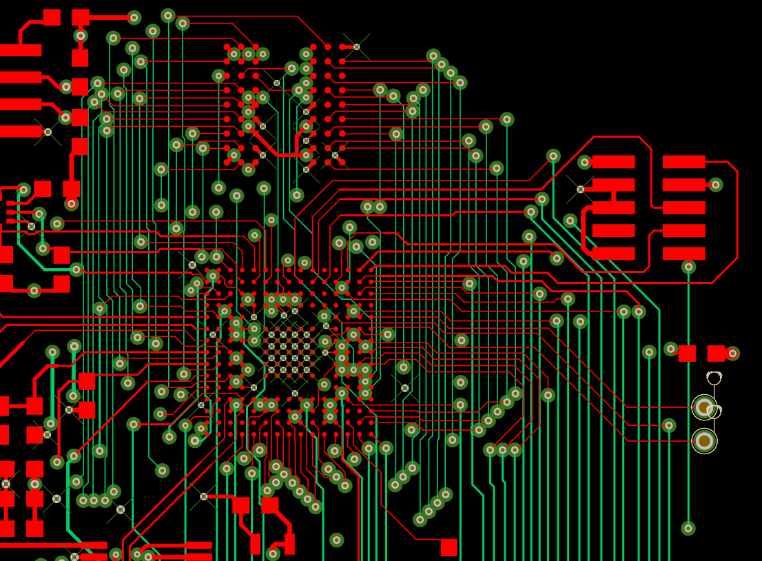
When laying out PCB design traces, start by separating power, ground, and signal lines to minimize noise. Power traces typically need more width to handle current without voltage sag, while signal traces prioritize short paths for digital integrity. Ground planes, large copper areas, complement traces by providing low-impedance returns and shielding. Hobbyists often use autorouters in free design software, but manual tweaks ensure optimal flow. Follow a logical order: route critical high-current paths first, then high-speed signals, and fill in the rest.
Layer stacking matters in multilayer boards, with signals sandwiched between power and ground planes for better performance. Through-hole vias connect layers reliably, but blind or buried vias save space in advanced hobby projects. Maintain consistent trace widths within net classes for uniform behavior. Angle traces at 45 degrees instead of 90 for smoother signal propagation and easier manufacturing. These PCB traces in PCB design techniques build robust boards step by step.
A PCB Trace Guide: Best Practices for Hobbyists
Follow these actionable steps in your PCB trace guide to elevate designs. First, calculate minimum widths using conservative rules: wider for power, narrower for low-current signals. Space traces at least three times the width apart to reduce crosstalk, especially near sensitive analog sections. Avoid running traces under large components that generate heat, as expansion can lift copper. Use teardrops at pad connections to prevent drill breakout during fabrication. For hobby prototypes, stick to 2-layer boards initially to master fundamentals before multilayer complexity.
Incorporate ground pours around traces to stabilize voltages and aid heat spreading. Test impedance informally by simulating in software for high-frequency hobbies like RF modules. Adhere to IPC-2152 principles for current handling to prevent trace burnout in motor drivers. Document your design rules for reuse across projects. These practices make what do PCB traces do reliable in real-world use.
Route differentially for balanced signals like USB or LVDS, twisting pairs virtually on the board. Review the layout with a DRC check for violations. Iterate with cheap prototypes to refine.
Common Challenges with PCB Traces and Troubleshooting
Hobbyists often face trace-related issues like delamination from poor adhesion or etching errors causing opens. Overly thin traces overheat under load, manifesting as dim components or resets. Crosstalk appears as erratic behavior in nearby digital lines. Manufacturing tolerances exacerbate narrow traces, leading to inconsistent widths. Thermal cycling warps boards, stressing traces at bends.
Troubleshoot by inspecting with a multimeter for continuity and a microscope for defects. Beef up suspect traces with jumper wires on prototypes. Redesign with wider margins for hobby fabs, which have looser tolerances than pro shops. IPC-A-600 outlines acceptability criteria for trace quality post-fabrication. Learn from failures to refine future PCB design traces.
Electromagnetic interference sneaks in via unshielded long traces; shorten or guard them. Simulate heat early to spot hotspots.
Conclusion
PCB traces form the vital conduits in every electronic project, enabling components to communicate and function as intended. This exploration of what are PCB traces highlights their design, properties, and best practices tailored for hobbyists. By applying a solid PCB trace guide, you enhance reliability and performance in PCB traces in PCB design. Experiment confidently, reference standards wisely, and iterate on prototypes. Your next hobby board will route flawlessly, bringing ideas to life efficiently.
Frequently Asked Questions
Q1: What are PCB traces and why do they matter in hobby projects?
A1: PCB traces are copper pathways on a circuit board that connect components by carrying electrical signals and power. In hobby projects, they matter because improper traces cause failures like signal loss or overheating, ruining prototypes. Understanding PCB traces in PCB design ensures your LED drivers or sensor circuits work reliably. Follow basic spacing and width rules for success.
Q2: What do PCB traces do in a typical PCB design?
A2: PCB traces conduct current between parts, distributing power and routing signals per the schematic. They replace wires for compactness and repeatability. In PCB design traces, they must handle varying loads without distortion. Hobbyists size them wider for batteries or motors to avoid drops.
Q3: How can I improve PCB design traces as a beginner?
A3: Start with wider traces and generous spacing in your PCB trace guide. Route power first, signals last, and use ground planes. Check continuity post-assembly. Reference IPC standards for guidance without specifics. Practice on simple 2-layer boards.
Q4: What common mistakes occur with PCB traces?
A4: Narrow traces for high current lead to heat issues, while tight spacing causes shorts. Sharp bends weaken joints. Hobbyists fix by reviewing layouts and using DRC tools. Proper planning in PCB traces in PCB design prevents most problems.
References
IPC-2221B — Generic Standard on Printed Board Design. IPC, 2009
IPC-2152 — Standard for Determining Current Carrying Capacity in Printed Board Design. IPC, 2009
IPC-A-600H — Acceptability of Printed Boards. IPC, 2010


