What is a Solder Mask Bridge in PCB Manufacturing?
A solder mask bridge, often referred to as a solder mask dam, is a deliberate application of solder mask material that acts as a physical barrier between adjacent solder pads or traces on a printed circuit board (PCB). Its primary purpose is to stop molten solder from inadvertently spreading and creating electrical shorts between these closely spaced conductive features during the soldering process.
This carefully designed separation is crucial for ensuring the electrical integrity of a PCB. Without these "dams," especially in boards with fine-pitch components, solder could easily flow across small gaps, leading to unintended electrical connections and circuit malfunctions. The presence of a bridge ensures solder stays precisely where it's needed.
How Does a Solder Mask Bridge Function During Soldering?
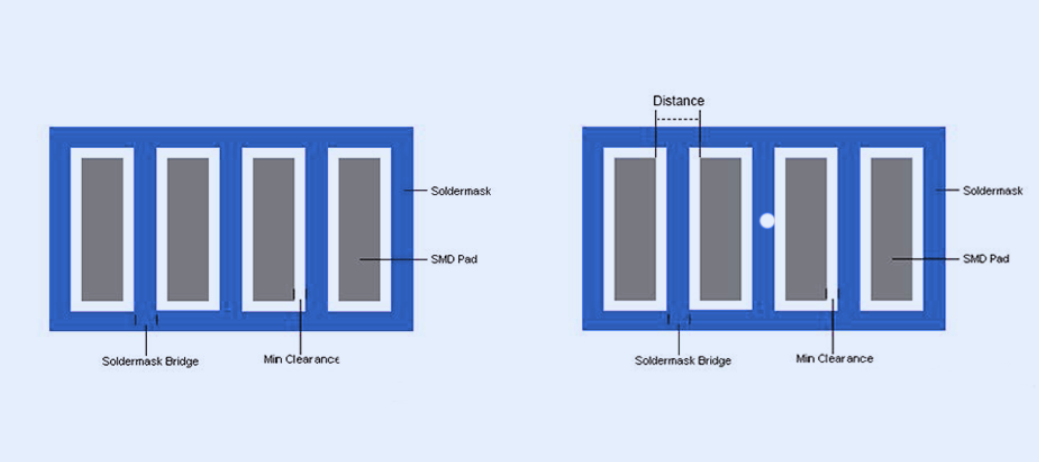
During PCB fabrication, a protective solder mask layer is applied across the entire board surface. It's then selectively removed from areas intended for soldering, such as component pads. When a design calls for a solder mask bridge, the mask material is intentionally left in place between two pads that are very close to each other.
Precision in Solder Placement
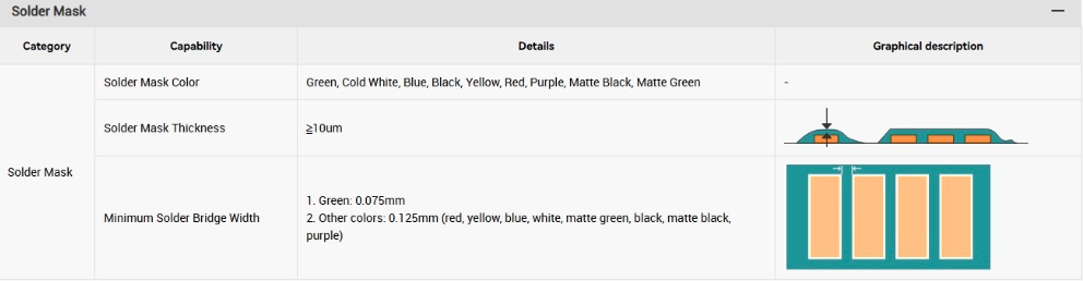
This bridge acts like a miniature wall, confining the solder to its respective pad during reflow or wave soldering. This precision is vital for surface-mount technology (SMT) components, particularly those with very fine lead pitches, where even a slight overflow of solder could bridge connections. The effectiveness of the bridge depends on its width and thickness, which are carefully controlled according to manufacturing capabilities and design specifications. Large pcb manufacturer like AIVON can produce very narrow bridges, sometimes as thin as 3-4 mils.
Design Considerations for Effective Bridges
For a solder mask bridge to be effective, the spacing between pads must be greater than the minimum bridge width achievable by the PCB manufacturer. If the gap is too small, a reliable bridge may not form, and designers might opt for an alternative approach, like a unified solder mask opening over both pads. Additionally, proper alignment of the solder paste stencil with the solder mask bridge is essential during assembly to ensure precise solder paste deposition.
What Are the Key Benefits of Using Solder Mask Bridges?
Solder mask bridges offer several important advantages in PCB assembly, significantly contributing to the reliability and efficiency of electronic devices.
Preventing Short Circuits
The most critical benefit is their role in preventing electrical short circuits. By physically isolating closely spaced pads, solder bridges effectively block the flow of solder between unintended points, which is particularly important for high-density designs with minimal spacing. This directly reduces the likelihood of board failures.
Enhancing Manufacturing Yield
By mitigating short circuits and ensuring more precise solder placement, solder mask bridges lead to higher manufacturing yields. Fewer defects mean less rework and fewer scrapped boards, which translates into cost savings and more efficient production processes. They eliminate the need for additional complex steps to manage solder flow in tight spaces.
Are There Any Limitations to Solder Mask Bridges?
While highly beneficial, solder mask bridges do have certain limitations that designers and manufacturers must consider.
Fabrication Constraints
The primary limitation is tied to manufacturing capabilities. Not all PCB fabricators can consistently produce extremely narrow solder mask bridges, especially for ultra-high-density designs. The precision required for very fine-pitch components might push the limits of some equipment and processes.
Potential for Thermal Stress
Though uncommon with advanced materials and processes, there is a slight possibility that a solder mask bridge could experience cracking or peeling due to thermal stress during the soldering process or subsequent operation. This risk is minimized by using high-quality solder mask materials and optimized thermal profiles.
How Do Solder Mask Bridges Fit into Overall PCB Design?
The concept of a solder mask bridge is just one facet of the broader solder mask layer's importance in PCB design and manufacturing. The solder mask, typically made from an epoxy-based polymer and most commonly green, serves multiple critical functions beyond preventing solder shorts.
It protects the delicate copper traces from environmental factors such as moisture, dust, and contaminants, thereby extending the board's lifespan. The solder mask also plays a role in the board's aesthetics. Designers must integrate solder mask bridge considerations into their overall design for manufacturability (DFM) strategies. This involves carefully balancing functional requirements with the practical limitations and capabilities of the fabrication and assembly processes, often using tools like Gerber files to ensure correct implementation.


