What Are Power Planes and Their Importance in PCB Design?
Fundamentals of Power Planes
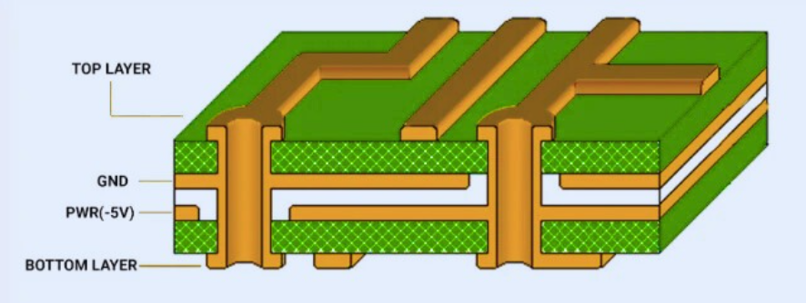
In the realm of printed circuit board (PCB) design, effective power distribution is fundamental to achieving optimal performance and unwavering reliability. A power plane is a dedicated conductive layer within a multilayer PCB, specifically engineered to distribute voltage to various components. Unlike individual traces, a power plane, often found in a 4-layer PCB stackup, offers a low-impedance pathway for current, which ensures consistent and stable power delivery across the entire board. This design approach significantly minimizes voltage drops and reduces electrical noise, attributes that are crucial for high-speed and mixed-signal designs.
Role in EMI Reduction and Signal Integrity
Power planes are typically paired with ground planes to establish a robust return path for signals, thereby further mitigating electromagnetic interference (EMI). This setup is critical for achieving EMI compliance. However, in intricate designs featuring multiple voltage levels or mixed-signal circuits, a single, undifferentiated power plane may prove insufficient. This is precisely where the concept of power plane segmentation becomes indispensable.
What is Power Plane Segmentation in PCBs?
Power plane segmentation, commonly referred to as "splitting," involves dividing a continuous power plane into distinct regions. Each region is then dedicated to supplying different voltages or isolating specific power domains. For example, in a mixed-signal PCB, one segment of the power plane might deliver 3.3V to digital components, while another section provides 5V to analog circuits. These segmented areas are physically isolated by deliberate gaps in the copper layer, effectively preventing unwanted electrical interference between the different power domains.
Splitting is frequently achieved using isolation techniques such as "moats" (gaps strategically placed within the plane) or by incorporating ferrite beads, which act as filters to suppress noise transfer between sections. The primary objective is to shield sensitive circuits, like analog sensors, from the noise inherently generated by high-speed digital components.
When Should You Consider Splitting Power Planes?
The decision to implement a split power plane is not universal; it hinges on the specific requirements of your project. Here are common scenarios where segmentation offers significant benefits:
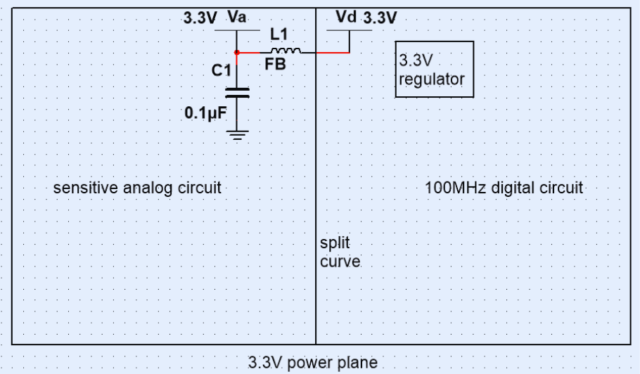
● Mixed-Signal PCBs: When a board integrates both analog and digital circuitry, splitting the power plane helps isolate noisy digital signals from sensitive analog components. For instance, a microcontroller switching at 100 MHz can generate noise that severely disrupts a precision analog-to-digital converter (ADC) operating nearby.
● Multiple Voltage Levels: If your design necessitates different voltages (e.g., 1.8V for low-power components and 5V for others), segmenting the power plane ensures that each section receives its correct voltage without detrimental interference.
● High-Speed Designs: In high-speed circuits, splitting can effectively reduce the cross-coupling of noise through the power plane, particularly when clock signals exceed 1 GHz, thereby preserving signal integrity.
● Noise-Sensitive Applications: For applications such as medical devices or high-fidelity audio equipment, where even minuscule amounts of noise can critically degrade performance, isolating power domains via splits is often a necessary design choice.
What Are the Advantages of Split Power Planes?
Splitting power planes provides several compelling benefits, particularly in complex or noise-sensitive designs.
Enhanced Noise Isolation and Reduced EMI
One of the foremost reasons for power plane segmentation is to significantly reduce noise. Digital circuits, characterized by their rapid-switching signals, generate substantial electrical noise that can readily couple into analog circuits if they share a common power plane. By splitting the plane, a physical barrier is created, which substantially minimizes this interference. For example, separating a digital 3.3V domain from an analog 5V domain can reduce noise coupling by up to 20 dB in certain designs. This isolation also restricts the spread of electromagnetic interference (EMI) across the board, proving invaluable in mixed-signal PCBs where digital switching noise could otherwise radiate and disrupt analog signals.
Improved Signal Integrity and Voltage Management
In high-speed designs, maintaining robust signal integrity is paramount. A segmented power plane reduces the risk of ground bounce and voltage fluctuations affecting adjacent circuits. This is especially critical for signals exceeding 500 MHz, where even minor impedance mismatches can lead to reflections and data corruption. Furthermore, modern PCBs frequently require multiple voltage levels. Splitting the power plane allows for dedicated regions for each voltage, simplifying power distribution. A system-on-chip (SoC), for instance, might require 1.2V for its core and 3.3V for I/O pins, a configuration easily managed with a split plane.
What Are the Disadvantages of Split Power Planes?
While splitting power planes offers clear advantages, it also introduces challenges. Understanding these drawbacks is essential for determining if this technique is appropriate for your specific design.
Increased Design Complexity and Potential for Return Path Issues
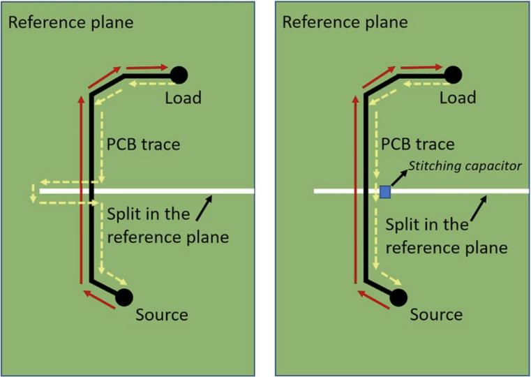
Splitting a power plane inevitably adds complexity to the PCB layout process. Careful planning is required for the placement of splits, ensuring proper routing of traces across these gaps, and strategically adding filtering components like ferrite beads or decoupling capacitors. This can extend design time and heighten the risk of errors, particularly in densely populated boards. A significant concern is the impact on signal return paths. If a signal trace crosses a split without an immediately adjacent ground plane for its return current, it can lead to signal integrity issues such as crosstalk or increased impedance. For example, a high-speed signal traversing a split might experience a return path impedance jump from 50 ohms to over 100 ohms, causing damaging reflections.
Higher Manufacturing Costs and Risk of Incomplete Isolation
Implementing split power planes often necessitates additional layers or more precise manufacturing processes, which can increase the overall custom PCB cost. While a standard four-layer board might suffice for a unified power plane, a split design may require meticulous alignment of splits and additional vias, potentially increasing fabrication expenses by 10-20% in some scenarios. Moreover, if not executed flawlessly, splitting can fail to fully isolate noise. For instance, if decoupling capacitors are not positioned optimally close to components (ideally within 0.1 inches), noise can still couple between domains through parasitic paths. This can negate the intended benefits of splitting and potentially degrade performance.
Best Practices for Effective Power Domain Isolation
If you opt to split your power plane, adhering to best practices is crucial to maximize benefits and minimize drawbacks.
Strategic Planning and Filtering Components
Align splits with the inherent boundaries of your circuit layout. For mixed-signal PCBs, strategically place digital components on one side of a split and analog components on the other. This minimizes the likelihood of signals traversing the split and disrupting critical return paths. To further enhance domain isolation, incorporate filtering components such as ferrite beads or inductors at the boundaries of split planes. These components function as high-frequency filters, effectively blocking noise while allowing DC power to pass unimpeded. A typical ferrite bead with an impedance of 600 ohms at 100 MHz can significantly reduce noise coupling between domains.
Ground Plane Integrity and Decoupling
While splitting power planes is often necessary, it is paramount to avoid segmenting the ground plane. A continuous ground plane provides a stable and consistent return path for all signals, which is vital for mitigating EMI and maintaining signal integrity. If a split ground plane becomes absolutely unavoidable, it must be implemented with meticulous planning and thorough simulation. Decoupling capacitors are indispensable for noise suppression in designs with split power planes. Place them as close as possible to the power pins of integrated circuits (ICs), ideally within 0.05 to 0.1 inches. Employ a diverse range of capacitance values (e.g., 0.1 μF and 1 μF) to effectively address a broad spectrum of noise frequencies.
Simulation and Rigorous Testing
Prior to finalizing your PCB design for manufacturing, leverage simulation tools to comprehensively analyze the impact of splits on signal integrity and noise characteristics. Advanced tools can accurately predict impedance mismatches or EMI issues, enabling you to refine split placements or component arrangements. Post-fabrication testing with an oscilloscope is also crucial for verifying noise levels, ensuring they remain well below acceptable thresholds, such as 50 mV peak-to-peak.
Are There Alternatives to Splitting Power Planes?
Splitting power planes is not always the optimal solution. Depending on your design's specific requirements, alternative techniques can achieve similar noise reduction and isolation benefits with potentially less complexity.
● Dedicated Power Supplies: Instead of segmenting a single power plane, utilize individual voltage regulators for different power domains. This approach offers complete electrical isolation without requiring modifications to the PCB layout itself.
● Optimized Component Placement: Group similar components together (e.g., all digital ICs in one designated area) to inherently minimize noise coupling, which can reduce or even eliminate the need for power plane splits.
● Enhanced Decoupling Networks: Implement a robust and comprehensive network of decoupling capacitors to effectively suppress noise across a unified power plane, thereby circumventing the necessity for segmentation.
Conclusion: Making the Right Choice for Your PCB Design
Power plane segmentation can be an exceptionally powerful technique for managing noise and isolating power domains in complex PCB designs, particularly in mixed-signal applications. The advantages of split power planes, such as enhanced noise isolation and superior signal integrity, often outweigh the associated drawbacks when executed correctly. However, challenges including increased design complexity and the potential for return path issues mean that it is not a universally applicable solution.
By meticulously planning splits, judiciously incorporating filtering components, and adhering to best practices for power domain isolation, you can ensure that your design operates with unwavering reliability. Whether you are developing a high-speed system or a noise-sensitive application, understanding precisely when and why to divide your PCB’s power plane is fundamental to achieving success. Carefully evaluate your project’s unique needs, simulate potential issues comprehensively, and then select the approach that strikes the optimal balance between performance requirements and practical implementation. With a well-conceived strategy, power plane segmentation can significantly elevate your PCB design, leading to cleaner power distribution and robust operation across diverse applications.


