Introduction
In the design of printed circuit boards (PCBs) for high current applications, ensuring reliable connections to ground and power planes is critical. Vias, small conductive pathways that link different layers of a PCB, play a vital role in maintaining signal integrity and managing thermal and electrical performance. For engineers working on power electronics, motor drivers, or high power systems, the decision to use multiple vias instead of a single via can significantly impact reliability and efficiency. This article explores the conditions under which multiple vias are necessary for connecting to ground or power planes in high current designs. By understanding the principles of current distribution, thermal management, and impedance control, designers can optimize their layouts for enhanced performance and durability while adhering to industry standards.
What Are Vias and Why Do They Matter in High Current Designs
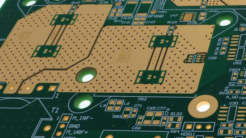
Vias are essential components in multilayer PCB designs, providing electrical and thermal connections between layers. In high current applications, vias facilitate the transfer of substantial electrical energy to power planes or ground planes, ensuring stable voltage levels and minimizing noise. Their importance lies in their ability to handle large currents without excessive voltage drops or overheating, which could compromise signal integrity and lead to system failures. Poor via design can result in increased resistance, localized hotspots, and electromagnetic interference (EMI), all of which degrade reliability. Therefore, selecting the appropriate number and configuration of vias is a fundamental aspect of PCB design for high current environments, directly influencing the board's overall performance and lifespan.
Technical Principles Behind Using Multiple Vias
Current Carrying Capacity and Resistance
The primary reason for using multiple vias in high current designs is to increase the current carrying capacity. A single via has a limited cross sectional area, which restricts the amount of current it can handle before encountering significant resistance. According to industry standards like IPC-2221B, Generic Standard on Printed Board Design, the current capacity of a via depends on its diameter, plating thickness, and material properties. Multiple vias connected in parallel effectively reduce the overall resistance of the path, allowing higher currents to flow without excessive voltage drops. This approach distributes the current load across several conductive paths, minimizing the risk of failure due to overcurrent in any single via.
Thermal Dissipation and Heat Management
High current flow generates heat due to resistive losses, and vias can become thermal bottlenecks if not designed properly. A single via may struggle to dissipate heat effectively, leading to elevated temperatures that can degrade surrounding materials or components. Multiple vias increase the surface area available for heat transfer, spreading thermal energy across a larger region. This is particularly important when connecting to ground planes, which often serve as heat sinks in multilayer boards. Proper via placement and quantity help maintain acceptable temperature levels, ensuring long term reliability in demanding applications.
Impedance Control and Signal Integrity
In high current designs, maintaining low impedance paths to power and ground planes is crucial for preserving signal integrity. A single via introduces inductance and resistance, which can cause voltage fluctuations or noise, especially at high frequencies. Multiple vias reduce the effective inductance by providing parallel paths, stabilizing the power delivery network. This is vital for circuits with fast switching components, where transient currents can induce unwanted noise. By strategically placing multiple vias, designers can minimize loop inductance and enhance the overall electrical performance of the PCB.
Related Reading: High Reliability Blind Via Design: Meeting Stringent Industry Standards
Practical Solutions for Implementing Multiple Vias
Determining the Number of Vias Needed
Calculating the required number of vias for a high current connection involves assessing the expected current load and the specifications of the via itself. Industry guidelines, such as those in IPC-2221B, provide formulas and tables to estimate current capacity based on via size and copper thickness. For instance, if a single via can safely carry a specific amount of current, designers can scale the number of vias proportionally to handle larger loads. It is also important to consider derating factors for thermal and environmental conditions to avoid overloading any single path.
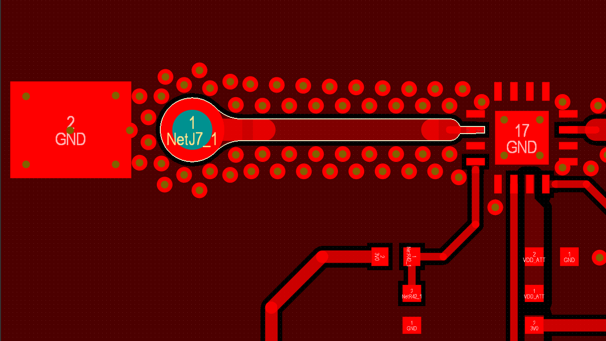
Placement Strategies for Optimal Performance
The placement of multiple vias is just as critical as their quantity. Vias should be positioned close to the components or pads requiring high current to minimize trace length and associated resistance. Arranging vias in a grid or array pattern can help distribute current evenly, reducing the risk of localized overheating. Additionally, placing vias near the edges of power planes or ground planes can enhance thermal dissipation by leveraging the larger copper area. Careful attention to via spacing ensures compliance with manufacturing constraints outlined in standards like IPC-6012E, Qualification and Performance Specification for Rigid Printed Boards.
Via Types and Manufacturing Considerations
Not all vias are identical, and selecting the appropriate type is essential for high current applications. Through hole vias offer robust connections across all layers, making them suitable for multilayer boards with extensive power planes. Blind and buried vias, while more complex to manufacture, can save space and improve routing efficiency in dense designs. Microvias, often used in high density interconnect (HDI) boards, may be less suitable for high current due to their smaller size, unless multiple are used. Designers must balance performance needs with manufacturing capabilities, adhering to guidelines in IPC-A-600K, Acceptability of Printed Boards, to ensure quality and reliability.
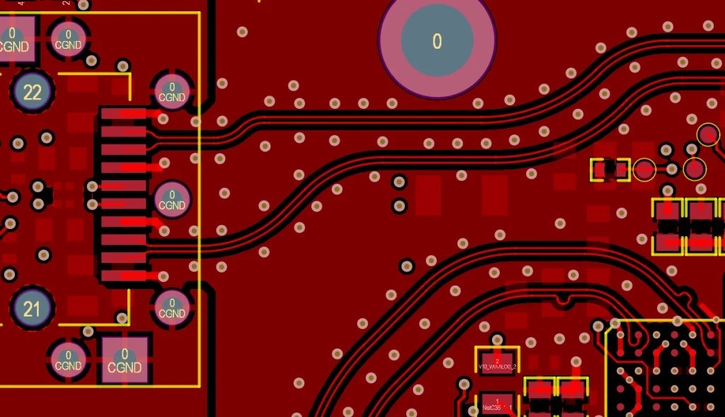
Stitching Vias for Enhanced Grounding
In addition to power connections, multiple vias are often used for stitching ground planes across layers. This technique, known as via stitching, creates a low impedance path for return currents, reducing EMI and improving signal integrity. Stitching vias are particularly useful in high speed and high current designs, where ground bounce can disrupt operation. Placing stitching vias at regular intervals around critical signal paths or power delivery areas helps maintain a consistent reference plane, as recommended in various industry resources focused on PCB layout practices.
Troubleshooting Common Issues with Vias in High Current Designs
Overheating and Thermal Stress
One common issue in high current PCB designs is overheating at via locations, often due to insufficient current capacity or poor thermal management. Engineers can address this by increasing the number of vias or using larger diameter vias to reduce resistance. Additionally, ensuring adequate copper thickness on power planes and ground planes, as specified in IPC-6012E, helps dissipate heat more effectively. Thermal simulations during the design phase can identify potential hotspots before manufacturing, allowing for adjustments in via count or placement.
Manufacturing Defects and Reliability Concerns
Manufacturing defects, such as incomplete plating or voids in vias, can compromise their performance in high current applications. Such defects increase resistance and reduce reliability, potentially leading to failures under load. Adhering to inspection criteria in IPC-A-600K ensures that vias meet quality standards for plating integrity and connection strength. Designers should also specify via fill materials or capping processes if needed, particularly for high reliability applications, to prevent issues like outgassing or cracking during thermal cycling.
Related Reading: The Impact of Via Design on PCB Prototyping: Minimizing Signal Loss and Maximizing Performance
Conclusion
Using multiple vias to connect to ground or power planes in high current PCB designs is a proven strategy for enhancing electrical performance, thermal management, and overall reliability. By distributing current load, reducing impedance, and improving heat dissipation, multiple vias address the challenges posed by high power applications. Engineers must carefully evaluate current requirements, via placement, and manufacturing constraints to optimize their designs. Following industry standards like IPC-2221B, IPC-6012E, and IPC-A-600K ensures that via implementations meet rigorous quality and performance criteria. With thoughtful design practices, multiple vias can significantly elevate the robustness and efficiency of PCBs in demanding environments.
FAQs
Q1: Why are multiple vias necessary for high current connections to power planes?
A1: Multiple vias are essential in high current designs to handle larger electrical loads by reducing resistance and increasing current capacity. A single via may overheat or fail under stress, compromising reliability. Using several vias in parallel distributes the current, minimizes voltage drops, and enhances thermal dissipation, ensuring stable connections to power planes as per guidelines in IPC-2221B.
Q2: How do multiple vias improve signal integrity in high current PCBs?
A2: Multiple vias lower the inductance and resistance of paths to ground planes and power planes, stabilizing voltage levels. This reduces noise and ground bounce, which are critical for maintaining signal integrity, especially in high speed circuits. Strategic placement of vias near critical components ensures minimal loop inductance, supporting clean signal transmission in demanding applications.
Q3: What factors determine the number of vias needed for ground planes in high current designs?
A3: The number of vias depends on the expected current load, via size, and copper thickness, as outlined in IPC-2221B. Environmental conditions and thermal constraints also influence the count. Designers calculate requirements based on current capacity per via and derate for safety, ensuring reliable connections to ground planes without risking overheating or failure.
Q4: How does via stitching enhance reliability in high current PCB layouts?
A4: Via stitching connects ground planes across layers, creating low impedance return paths for currents. This technique reduces EMI and improves reliability by minimizing noise in high current designs. Regular placement of stitching vias around power delivery areas ensures consistent grounding, supporting stable operation and adherence to best practices for multilayer boards.
References
[IPC-2221B — Generic Standard on Printed Board Design. IPC, 2012.]
[IPC-6012E — Qualification and Performance Specification for Rigid Printed Boards. IPC, 2020.]
[IPC-A-600K — Acceptability of Printed Boards. IPC, 2020.]


