Introduction
Internet of Things (IoT) devices demand PCBs that prioritize compactness, energy efficiency, and seamless wireless performance. In IoT PCB design 1 oz copper emerges as an optimal choice, offering sufficient conductivity for low-power applications without the added bulk or cost of thicker foils. Electrical engineers often select this standard thickness to support small PCB design while maintaining manufacturability and reliability. This article delves into the engineering rationale behind using 1 oz copper, outlines critical design considerations, and shares best practices tailored for wireless PCB design and low-power PCB design. By adhering to established principles, designers can mitigate risks like signal degradation or mechanical instability in constrained form factors.
The shift toward battery-operated sensors, wearables, and smart modules underscores the need for precise PCB engineering. 1 oz copper, equivalent to 35 micrometers in thickness, aligns perfectly with these requirements, enabling finer trace geometries essential for high-density layouts. Engineers must balance electrical performance with fabrication tolerances to ensure devices operate reliably in diverse environments.
Understanding 1 oz Copper in PCB Fabrication
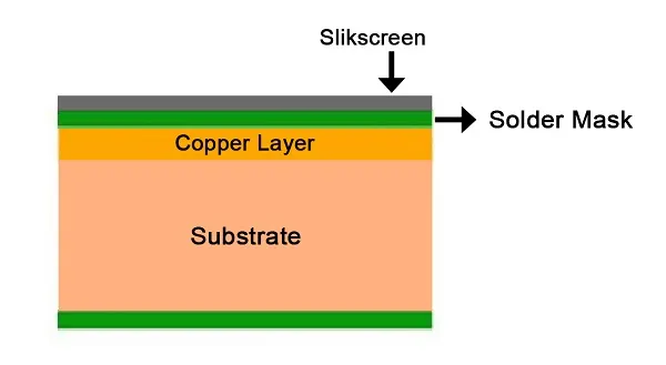
1 oz copper refers to a foil weight of one ounce per square foot, translating to a nominal thickness of 35 micrometers after plating. This specification is the de facto standard for most rigid PCBs due to its versatility in etching processes and compatibility with common substrates like FR-4. Thinner foils allow for tighter trace widths and spaces, which is crucial in achieving the miniaturization goals of modern electronics. Fabrication begins with lamination of copper to prepreg and core materials, followed by imaging, etching, and plating to build up the circuit pattern.
In the context of IoT, this copper weight supports the transition from prototype to production without necessitating specialized heavy-copper processes. The uniformity of 1 oz foil ensures consistent impedance across traces, vital for high-frequency signals in wireless modules. Engineers should verify copper distribution during design review to prevent variations that could affect yield.
Why 1 oz Copper Excels in IoT Applications
IoT devices typically operate at low currents, often below 500 milliamperes, making the conductivity of 1 oz copper more than adequate for power distribution. Thicker coppers, such as 2 oz or higher, introduce unnecessary rigidity and etching challenges, increasing costs and board thickness. For low-power PCB design, 1 oz enables efficient routing of sleep-mode circuits and intermittent high-speed bursts without excessive voltage drop. This choice also facilitates small PCB design by allowing higher component density on limited real estate.
Wireless connectivity in IoT relies on stable RF paths, where 1 oz copper provides low enough resistance for antennas and matching networks at frequencies like 2.4 GHz or sub-GHz bands. The thinner profile reduces parasitic inductance in vias and traces, improving signal integrity over short distances. Moreover, it aligns with sustainability goals by minimizing material use while meeting performance thresholds.
Mechanical properties further favor 1 oz in compact enclosures. The foil's flexibility aids in thermal expansion matching with dielectrics, reducing stress during assembly reflow. Overall, this copper weight strikes an ideal balance for devices prioritizing longevity on coin-cell batteries or energy harvesting.
Key Design Considerations for 1 oz Copper PCBs
Trace Routing and Current Capacity
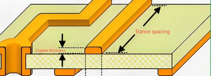
Engineers must calculate trace widths meticulously to handle expected currents without exceeding temperature rise limits. IPC-2221 provides guidelines for determining minimum widths based on copper thickness, ambient temperature, and allowable delta-T. For external layers in 1 oz copper, wider traces compensate for external convection cooling compared to internal planes. In IoT PCB design 1 oz copper, prioritize conservative sizing for power traces to account for peak loads during data transmission.
Routing density increases with finer features possible on 1 oz foil, but spacing rules prevent shorts during etching undercut. Differential pairs for serial protocols demand controlled widths to maintain impedance. Always simulate thermal profiles to validate designs under worst-case scenarios.
Signal Integrity in Wireless PCB Design
High-speed interfaces in wireless PCB design require controlled dielectric thickness and trace geometry to achieve 50-ohm or 100-ohm impedances. 1 oz copper's uniformity supports microstrip and stripline configurations effectively at IoT frequencies. Minimize vias in RF paths to preserve insertion loss, opting for blind or buried types where layers permit. Ground pour stitching enhances return paths, reducing EMI susceptibility common in battery-powered nodes.
Crosstalk becomes a concern in dense small PCB design; length-matching and serpentine routing mitigate skew. Pre-layout stackup analysis ensures consistent propagation delays across the board.
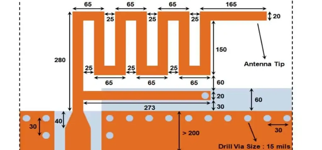
Antenna Design with 1 oz Copper
Antenna design 1 oz copper demands clear keep-out zones free of copper fills or components to optimize radiation patterns. Common types like inverted-F or meander line antennas fit well on board edges, leveraging the foil's conductivity for quarter-wave elements. Matching networks use series inductors and shunt capacitors tuned via simulation to account for nearby ground effects. The thinner copper minimizes surface waves that distort patterns in compact layouts.
Placement away from metal shields or batteries preserves efficiency; engineers should allocate at least lambda/4 clearance where possible. Post-layout EM simulation verifies VSWR below 2:1 across operating bands. Fabrication tolerances on 1 oz etching directly impact resonance, so specify tight line-width control.
Mechanical and Thermal Factors in Small PCB Design
Small PCB design amplifies warpage risks due to asymmetric copper distribution in thin stacks. Balanced layer pairing and core selection counteract bow and twist. Vias and pads consume disproportionate area, so optimize drill sizes per board thickness. Thermal vias under power ICs dissipate heat effectively with 1 oz pours, preventing hotspots in low-power PCB design.
IPC-6012E outlines qualification tests for warpage and registration, ensuring boards meet class 2 or 3 criteria for IoT reliability. Solder mask thickness over traces protects against handling damage without altering impedances significantly.
Best Practices for Optimal Performance
Select low-loss dielectrics with Dk around 4.0-4.5 for RF sections to minimize attenuation. Stackups typically feature 2-4 layers: signal-ground-signal-power for isolation. IPC-A-600 defines acceptability criteria for plating voids and etch quality, guiding fab specs. Incorporate test points and fiducials for automated assembly alignment in panelized small PCB design.
For low-power PCB design, segment power domains with ferrite beads to isolate noise. Solder mask dams prevent bridging on fine-pitch BGAs common in IoT SoCs. Final gerber reviews should confirm annular ring integrity around vias.
Adopt symmetric stackups to equalize CTE mismatches, enhancing reliability post-reflow. Dry film photoresist processes yield superior definition on 1 oz copper versus liquid methods.
Prototype iteratively with breadboard carriers to validate antenna tuning before full spin. Document rationale for trace widths in design files for future audits.
Troubleshooting Common Issues
Excessive insertion loss in wireless paths often stems from unstitched grounds; add vias every lambda/20. If boards exhibit delamination, verify prepreg flow during lamination per IPC-6012E. Antenna detuning post-assembly points to mechanical shifts; secure with underfill if flexing occurs.
Overheating traces indicate undersized widths; recalculate per IPC-2221 charts. Warpage in small PCB design resolves with edge beveling or carrier tabs during fab.
Conclusion
1 oz copper PCBs enable electrical engineers to craft efficient, compact IoT solutions balancing cost, size, and performance. Key considerations like trace sizing per IPC-2221, impedance control, and antenna isolation ensure robust wireless PCB design. Best practices in stackup symmetry and DFM minimize risks in low-power PCB design. By integrating these principles, teams achieve reliable small PCB design ready for volume production. Future IoT evolution will likely reinforce 1 oz as the go-to for edge devices.
FAQs
Q1: What are the main advantages of 1 oz copper in IoT PCB design?
A1: 1 oz copper supports IoT PCB design 1 oz copper by enabling narrow traces for high density and low resistance suitable for currents under 1 ampere. It reduces board thickness for small PCB design while maintaining etch precision. This choice excels in low-power PCB design, minimizing battery drain and heat. Standards like IPC-2221 guide sizing for optimal performance.
Q2: How does 1 oz copper impact wireless PCB design?
A2: In wireless PCB design, 1 oz copper provides consistent impedance for RF traces and low loss at IoT frequencies. Antenna design 1 oz copper benefits from edge placement and clear keep-outs to maximize efficiency. Thinner foil lowers parasitics, aiding matching networks. Engineers achieve better signal integrity without heavy copper rigidity.
Q3: What challenges arise in small PCB design with 1 oz copper?
A3: Small PCB design with 1 oz copper risks warpage from copper imbalance, addressed by symmetric stacks. Fine features demand tight fab tolerances for registration. Thermal management relies on vias rather than thick pours. IPC-A-600 ensures visual acceptability post-production.
Q4: Can 1 oz copper handle low-power PCB design requirements?
A4: Yes, low-power PCB design thrives on 1 oz copper for efficient power routing in sleep-active cycles. It supports segmented domains to curb noise. IPC-6012E verifies endurance under thermal cycling. This setup optimizes for energy harvesting or coin-cell operation.
References
IPC-2221B - Generic Standard on Printed Board Design. IPC, 2009
IPC-6012E - Qualification and Performance Specification for Rigid Printed Boards. IPC, 2017
IPC-A-600K - Acceptability of Printed Boards. IPC, 2020