Introduction
In the world of printed circuit board design and manufacturing, copper thickness plays a pivotal role in balancing performance and budget constraints. A 2oz copper PCB features copper foil that weighs 2 ounces per square foot, translating to approximately 70 microns in thickness, double that of the standard 1oz copper at 35 microns. Electrical engineers often face the dilemma of whether the enhanced capabilities of thicker copper justify the added expense in PCB manufacturing cost. This analysis delves into the 2oz copper PCB cost factors, compares it against standard options, and evaluates if the performance gains make it a worthwhile investment for high-demand applications. Factory insights reveal that while initial premiums exist, long-term reliability can offset them in power-intensive designs. Understanding these trade-offs ensures informed decisions aligned with project requirements.
What Is a 2oz Copper PCB and Why Does It Matter?
A 2oz copper PCB uses heavier copper cladding on one or both sides of the board, providing superior electrical and thermal properties compared to lighter weights. This thickness is specified during the design phase and must meet acceptability criteria outlined in IPC-A-600, which defines visual and dimensional standards for printed boards. Engineers select 2oz copper for applications demanding high current handling, such as power supplies, motor drives, and automotive electronics, where standard 1oz boards may overheat or require wider traces. The relevance stems from modern trends toward compact, high-power density designs that push the limits of conventional PCBs. Without adequate copper thickness, voltage drops and thermal hotspots compromise reliability, leading to failures in field deployments. Factory processes treat 2oz boards differently to maintain integrity, influencing overall PCB material cost.
In high-reliability sectors, 2oz copper reduces the need for additional layers or vias, streamlining multilayer stackups. It aligns with qualification requirements in IPC-6012 for rigid printed boards, ensuring consistent performance under stress. Procurement teams appreciate how this choice impacts PCB cost comparison across prototypes and production runs.
Technical Principles Behind 2oz Copper Performance
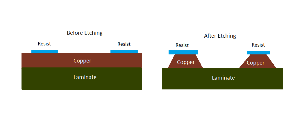
The core advantage of 2oz copper lies in its doubled cross-sectional area, which directly lowers electrical resistance per IPC-2152 guidelines for current-carrying capacity. Thicker traces carry approximately twice the current of 1oz equivalents at the same temperature rise, minimizing I^2R losses in power paths. This principle is critical for applications exceeding 10A per trace, where 1oz copper would demand excessively wide conductors, consuming valuable board real estate. Thermal conductivity improves as well, with copper's high thermal coefficient aiding heat spreading across the plane. During operation, this prevents localized hotspots that could delaminate the substrate or degrade components.
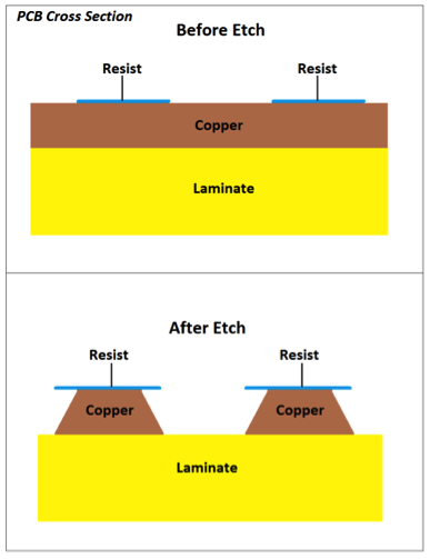
Manufacturing challenges arise from the etching process, as thicker copper etches slower and risks undercutting if panel exposure times are not precisely controlled. Factories compensate with differential etching techniques, adding steps that elevate PCB manufacturing cost. Warpage potential increases due to asymmetric thermal expansion between copper and FR-4 laminate, necessitating symmetric stackups in multilayer designs. Adherence to J-STD standards for handling and baking mitigates moisture-related issues exacerbated by heavier foils.
PCB Cost Breakdown: Material and Manufacturing Factors
PCB material cost for 2oz copper starts higher due to the increased volume of copper foil required per panel. Standard 1oz foil is commodity-priced, while 2oz demands specialized rolling and treatment, reflecting in raw laminate expenses. This premium compounds in high-volume orders, where every square meter counts toward total project budgets. Engineers conducting PCB cost comparison note that material alone can represent 20 to 40 percent of the difference between 1oz and 2oz prototypes.
Manufacturing processes amplify the 2oz copper PCB cost through extended cycle times. Etching thick copper requires finer chemistry control and longer immersion, potentially doubling panel processing duration compared to 1oz. Additional plating may be needed for vias to match outer layer robustness, introducing electroless and electrolytic steps. Surface finishes like ENIG or HASL must adapt to the rougher profile of heavier copper, sometimes necessitating extra smoothing. These factors collectively drive up labor and equipment utilization charges.
Pressing and lamination see elevated pressures to bond thicker foils without voids, per IPC-6012 performance specs. Electrical testing verifies continuity under higher current loads, adding probe wear and setup time. For complex boards, routing bits dull faster against denser copper, increasing tool replacement frequency.
- Raw Material: 1oz - Baseline pricing for standard foil; 2oz - Higher due to doubled thickness.
- Etching Process: 1oz - Standard speed and chemistry; 2oz - Slower etch rates, precise control needed.
- Plating and Finishing: 1oz - Routine application; 2oz - Adapted for rougher surface, potential extra steps.
- Testing and Inspection: 1oz - Basic continuity checks; 2oz - Enhanced for high-current validation.
- Yield Considerations: 1oz - Higher yields typical; 2oz - Slightly lower due to warpage risks.
Performance vs. Cost: Is 2oz Worth the Premium?
Performance metrics favor 2oz copper in scenarios where thermal management dictates longevity. Enhanced heat dissipation allows components to operate closer to rated specs without forced cooling, reducing system-level expenses like fans or heatsinks. In PCB cost comparison, this translates to fewer redesign iterations for overheating issues common in 1oz high-power boards. Reliability data from field applications shows lower failure rates in power electronics, justifying the upfront PCB manufacturing cost for mission-critical products.
However, for signal integrity-focused designs under 5A, 1oz suffices with wider traces, avoiding the premium altogether. Factory-driven insights highlight that 2oz shines in single-sided power planes, cutting layer count by consolidating functions. Diminishing returns apply beyond 2oz, as 3oz or heavier escalate costs exponentially without proportional gains unless currents exceed 50A.
Warpage control remains a key differentiator. Balanced copper weights across layers, as recommended in IPC-A-600, prevent bow and twist during reflow soldering. This ensures assembly yields match those of standard boards, preserving the cost-performance equation.
Best Practices for Specifying 2oz Copper PCBs
Select 2oz copper judiciously by calculating trace widths via IPC-2152 charts, factoring in rise-over-run ratios for your ambient temperatures. Communicate stackup symmetry early to fabricators, specifying outer layers consistently to minimize warpage below 0.75% per IPC standards. Opt for panelized designs in prototypes to amortize setup costs across multiples.
During procurement, request DFM feedback on etching feasibility, as trace-to-space ratios tighten with thickness. For multilayer boards, plane inner layers at 1oz unless full heavy copper is mandated, optimizing PCB material cost. Bake boards pre-assembly per JEDEC J-STD-020 to expel moisture trapped in thicker foils.
Validate prototypes with thermal cycling tests simulating end-use conditions. This confirms the performance premium delivers ROI through extended MTBF. Collaborate with suppliers on via filling techniques for interlayer reliability.
Conclusion
The 2oz copper PCB cost premium stems from elevated material demands and intricate manufacturing processes, yet it delivers unmatched current handling and thermal resilience for demanding applications. Electrical engineers benefit from structured evaluations weighing PCB cost comparison against operational gains, often finding value in power-dense designs. Adhering to IPC standards ensures quality without excess expenditure. Ultimately, 2oz proves worthwhile when standard options falter, aligning factory capabilities with engineering needs for robust outcomes.
FAQs
Q1: What factors most influence 2oz copper PCB cost?
A1: Material pricing for thicker foil and extended etching times dominate PCB manufacturing cost. Complex surface finishes and enhanced testing for high-current integrity add layers. Yields may dip slightly from warpage risks, but symmetric designs mitigate this. Overall, expect a noticeable premium over 1oz in PCB cost comparison.
Q2: How does 2oz copper affect PCB manufacturing cost compared to 1oz?
A2: Thicker copper demands specialized processes like controlled etching and plating, elevating labor and time inputs. Factories adjust chemistry for uniform removal, increasing operational expenses. While material cost rises directly with weight, process adaptations represent the larger share in total PCB manufacturing cost.
Q3: When is a 2oz copper PCB worth the extra PCB material cost?
A3: Choose 2oz for applications over 10A per trace requiring compact footprints and superior heat spreading. It reduces layer counts and enhances reliability per IPC-2152. For low-power signals, stick to 1oz to optimize budgets without performance loss.
Q4: Can 2oz copper PCBs reduce overall system costs despite higher upfront pricing?
A4: Yes, by enabling smaller boards and eliminating auxiliary cooling, long-term savings accrue. Fewer failures from thermal stress lower warranty claims. In high-volume power electronics, the PCB cost comparison favors 2oz for lifecycle value.
References
IPC-A-600K - Acceptability of Printed Boards. IPC, 2020
IPC-6012E - Qualification and Performance Specification for Rigid Printed Boards. IPC, 2017
IPC-2152 - Standard for Determining Current Carrying Capacity of Printed Board Traces. IPC, 2009