Introduction
Multilayer PCB routing forms the backbone of modern electronic designs, especially as hobbyists tackle more complex projects like microcontrollers, sensors, and wireless modules. Unlike single or double-layer boards, multilayer PCBs stack multiple copper layers separated by insulating materials, allowing for denser connections and better performance. For electronic hobbyists transitioning from simple prototypes, mastering multilayer PCB routing unlocks possibilities in compact, high-speed circuits. This guide serves as a multilayer routing tutorial, breaking down PCB layout essentials into beginner-friendly steps. You will learn PCB routing techniques that ensure reliable signal flow while avoiding common pitfalls. By the end, you will feel confident planning your next multilayer project.
What Are Multilayer PCBs and Why Does Routing Matter?
Multilayer PCBs consist of three or more conductive layers bonded together with prepreg and core materials, enabling intricate routing multilayer schemes. Hobbyists often start with two-layer boards for basic circuits, but multilayer designs become essential for projects requiring power distribution, signal isolation, and ground planes. Routing in these boards involves planning trace paths across layers, using vias to jump between them, which directly impacts signal integrity and electromagnetic compatibility. Poor multilayer PCB routing can lead to crosstalk, noise, or even board failure under load. Understanding why it matters helps hobbyists prioritize layout decisions early. Proper techniques align with industry practices, reducing iterations during prototyping.
Key Technical Principles of Multilayer PCB Routing
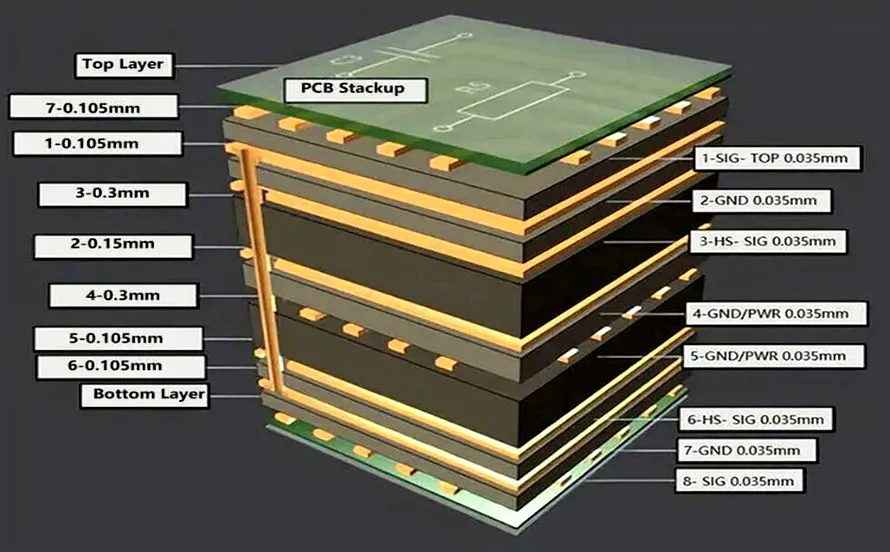
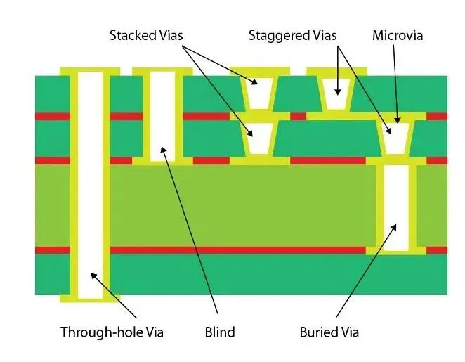
The foundation of multilayer PCB routing lies in the stackup, which defines layer order and material thicknesses for controlled impedance. Signal layers alternate with power and ground planes to minimize loop inductance and provide return paths for currents. In PCB layout, hobbyists must consider via types: through-hole vias connect all layers, while blind and buried vias save space in dense designs. Trace width and spacing follow rules based on current capacity and voltage to prevent overheating or arcing. IPC-2221 provides guidelines for these parameters, ensuring designs meet basic reliability thresholds. Electromagnetic fields between traces demand careful planning to avoid coupling in high-frequency signals.
Layer pairing affects differential signaling, where pairs route on adjacent layers for balanced impedance. Ground planes act as shields, but splitting them requires stitching vias to maintain continuity. Hobbyists should visualize current flow: signals seek the shortest low-impedance path back to ground. Ignoring this leads to ground bounce in multilayer routing. Thermal management also plays a role, as inner layers dissipate heat differently than outer ones. These principles guide every routing decision.
Essential PCB Routing Techniques for Multilayer Boards
Start multilayer PCB routing by defining a stackup suited to your project's speed and density, typically 4 to 8 layers for hobbyist applications. Use manual routing for critical nets like clocks or high-speed data, reserving autorouters for power floods. In PCB layout software, set design rules for minimum trace width, clearance, and via size based on your fabrication capabilities. Route high-speed signals first on inner layers, keeping them short and perpendicular to adjacent traces to reduce crosstalk. Employ length matching for data buses to prevent timing skew. These PCB routing techniques form a multilayer routing tutorial in action.
Vias introduce inductance, so minimize their use and fan out pads properly. For power distribution, pour copper planes and connect with multiple vias for low resistance. Hobbyists benefit from 45-degree bends over 90-degree corners to ease manufacturing and reduce reflections. Differential pairs require equal lengths and spacing, routed as twins. Ground vias near signal vias provide shielding. Practice these steps iteratively, reviewing DRC violations after each pass.
Best Practices for Routing Multilayer PCBs
Follow a systematic workflow: import your schematic, place components symmetrically for balanced routing, then assign layers logically. Dedicate outer layers to components and power entry, inner layers to signals and planes. Maintain consistent trace widths across nets of similar current, consulting IPC-6012 for performance specs on layer alignment. Space sensitive traces at least 3 times the dielectric thickness from planes to control impedance. Use teardrops at via-trace junctions to strengthen connections against drill wander. These multilayer PCB routing best practices minimize defects.
Address crosstalk by routing parallel traces on different layers or adding ground traces between them. For mixed-signal boards, segregate analog and digital sections with ground splits, stitching across splits with vias. Simulate impedance if possible, targeting 50 ohms for single-ended signals. Review fanout for BGA or fine-pitch parts early, as multilayer routing demands escape routes. Finally, perform a design review: check for loops, acute angles, and unconnected nets. Hobbyists iterating prototypes save time with these habits.
Common pitfalls include overusing vias, leading to higher resistance, or neglecting plane clearance around pads. Troubleshoot by exporting Gerber files and inspecting layers visually. Adjust stackup if impedance mismatches occur, thickening dielectrics or widening traces. For hobbyist budgets, aim for standard 1.6mm total thickness. J-STD-001 outlines soldering considerations that influence routing choices, like pad sizes. Persistent issues often trace back to schematic errors, so verify pin assignments first.
Troubleshooting Multilayer Routing Challenges
Hobbyists frequently encounter signal integrity issues in multilayer designs, such as ringing from unmatched impedances. Measure trace lengths and add series resistors if needed for termination. Crosstalk appears as noise on scopes; separate aggressor and victim traces across layers. Power plane splits cause voltage drops, fixed by adding decoupling caps near ICs and stitching vias. Warpage from uneven copper distribution warps boards, balanced by mirroring pours on opposite layers.
Fabrication feedback highlights drill breakout or plating voids from poor via annular rings. Enlarge clearances around slots or odd shapes. For high-layer counts, verify sequential lamination aligns cores properly. Hobbyist troubleshooting focuses on iterative testing: build, probe, reroute. Document changes to refine future multilayer routing tutorials.
Conclusion
Mastering multilayer PCB routing empowers electronic hobbyists to build professional-grade circuits with confidence. From stackup planning to via optimization, each PCB routing technique contributes to reliable performance. Prioritize signal integrity, follow design rules, and leverage standards for consistency. Practice on simple 4-layer boards before scaling up. With these insights, your next project will route smoothly, avoiding costly respins. Embrace multilayer possibilities and iterate toward perfection.
FAQs
Q1: What are the basic steps in a multilayer routing tutorial for beginners?
A1: Begin with schematic import and component placement in your PCB layout tool. Define stackup and design rules for traces, vias, and clearances. Route critical signals first on inner layers, then power planes, and fill with autorouting. Run DRC checks, review visually, and export Gerbers. This structured approach ensures clean multilayer PCB routing.
Q2: How do PCB routing techniques differ for multilayer vs. double-layer boards?
A2: Multilayer boards use inner planes for shielding and power, requiring vias for interlayer jumps, unlike surface-only double-layer routing. Maintain impedance with layer-specific widths and spacing in multilayer designs. Blind vias save space in dense areas absent in simpler boards. These adaptations enhance signal quality in complex hobbyist projects.
Q3: Why is via management crucial in routing multilayer PCBs?
A3: Vias add inductance and resistance, slowing signals and raising losses in multilayer routing. Limit their number, use arrays for power, and ensure adequate annular rings per IPC guidelines. Blind and buried types reduce stub effects for high-speed nets. Proper management preserves integrity across layers.
Q4: What common mistakes should hobbyists avoid in multilayer PCB routing?
A4: Avoid 90-degree bends causing reflections, uneven copper leading to warpage, and neglecting ground stitching across splits. Route parallels too close invites crosstalk. Overlook fanout for dense parts blocks escapes. Check these early to streamline PCB layout.
References
IPC-2221B — Generic Standard on Printed Board Design. IPC, 2009
IPC-6012E — Qualification and Performance Specification for Rigid Printed Boards. IPC, 2015
J-STD-001H — Requirements for Soldered Electrical and Electronic Assemblies. IPC, 2018


