Introduction
Multilayer printed circuit boards form the backbone of most advanced electronic devices, stacking multiple layers of conductive traces separated by insulating materials. For electronics hobbyists dipping their toes into beginner PCB projects, transitioning from single or double-sided boards to multilayer designs unlocks the potential for more compact and complex circuits. This guide walks you through the essentials of multilayer PCBs, from understanding their structure to navigating the PCB design process and manufacture stages. Whether you are prototyping a custom controller or experimenting with signal integrity challenges, mastering these boards elevates your hobbyist endeavors. By the end, you will have practical insights to integrate them confidently into your circuit board design workflows.
What Are Multilayer PCBs and Why Do They Matter for Electronics Hobbyists?
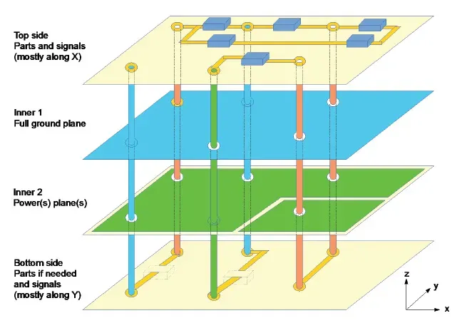
A multilayer PCB consists of three or more conductive layers, typically copper, bonded together with prepreg and core materials to create a single rigid board. Unlike simpler single-layer boards where all traces run on one side, multilayer designs route signals on inner layers, enabling higher component density and reduced electromagnetic interference. Electronics hobbyists benefit from this complexity when projects demand tight spacing, such as in wearable tech or multi-function Arduino shields. The ability to dedicate layers for power, ground, and signals separately improves performance and reliability in noisy environments. For beginners, starting with 4-layer boards strikes a balance between affordability and capability, avoiding the overwhelm of 8-layer or higher stacks common in professional gear.
These boards matter because modern hobby projects often outgrow basic layouts, leading to crosstalk or power delivery issues on simpler designs. Multilayer construction follows established layering principles that hobbyists can leverage without deep expertise. Cost has dropped significantly, making prototype runs accessible through standard PCB manufacture services. Understanding their relevance empowers you to choose the right board type early in the circuit board design phase, saving time and frustration down the line.
The Basics of the PCB Design Process for Multilayer Boards
The PCB design process begins with schematic capture, where you map out components and connections using beginner-friendly software tools. Once the netlist is generated, transition to layout by assigning signals to specific layers, starting with power and ground planes on inner layers for stability. Hobbyists should prioritize via placement next, as these interconnect layers and consume board real estate if overused. Route high-speed signals on outer layers for easier probing during testing, while keeping sensitive analog traces isolated. Iterating through design rule checks ensures trace widths meet current-carrying needs and clearances prevent shorts.
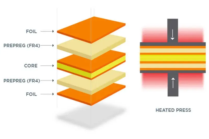
Layer stackup planning is crucial in multilayer circuit board design, defining the sequence of cores, prepregs, and foils that dictate impedance and thermal behavior. Beginners often model a symmetric stackup, like signal-ground-signal-power, to minimize warpage during fabrication. Simulate signal integrity early to spot issues like reflections from impedance mismatches. Export Gerber files and drill data only after a final review, preparing files for PCB manufacture. This structured approach keeps the process manageable for electronics hobbyists tackling their first multilayer beginner PCB.
Key Technical Principles Behind Multilayer PCBs
Multilayer PCBs rely on precise lamination, where alternating copper foils and dielectric sheets are pressed under heat and pressure to form a monolithic structure. Vias serve as the primary interconnects, with through-hole types piercing all layers, blind vias stopping at inner ones, and buried vias linking only internals for density. Material selection focuses on FR-4 for cost-effective hobby use, offering a balance of rigidity and low dielectric constant around 4.5. Copper thickness, typically 1 oz per square foot, influences current capacity and heat dissipation across layers.
Thermal management emerges from the stackup, as inner layers act as heat spreaders but can trap warmth if vias are sparse. Signal propagation speed depends on dielectric thickness and material properties, guiding trace length matching for hobbyist RF experiments. Mechanical integrity ties to board thickness, usually 1.6 mm for standard panels, preventing flex during handling. Adhering to these principles ensures reliable performance in beginner PCB applications.
Insights into Multilayer PCB Manufacture
PCB manufacture for multilayer boards starts with inner layer etching, where photoresist patterns define traces on copper-clad laminates. Panels then undergo black oxide treatment for better adhesion before lamination in an autoclave, fusing layers per IPC-6012E specifications for rigid printed boards. Outer layers receive similar etching after drilling, followed by plating to fill vias with copper. Solder mask application protects traces, and silkscreen adds component legends for assembly ease.
Quality control inspects for defects like delamination or voids using IPC-A-600K acceptability criteria, ensuring hobbyist prototypes meet baseline standards. Final steps include electrical testing for opens and shorts, plus routing to shape. Electronics hobbyists appreciate controlled impedance options during ordering, vital for USB or Ethernet signals. Manufacture tolerances, such as +/-0.1 mm for hole positions, directly impact fit in your projects.
Warpage control during cooling relies on balanced copper distribution across layers, a factory-driven practice to avoid assembly headaches. For beginner PCBs, opting for standard lead times balances cost and lead-free finishes like HASL or ENIG.
Best Practices for Designing and Using Multilayer PCBs as a Hobbyist
Start your multilayer PCB design process by sketching the stackup on paper, allocating ground planes adjacent to signal layers for shielding. Use 0.1-0.2 mm trace widths for hobby currents under 1A, widening for power rails to prevent overheating. Place decoupling capacitors near ICs on the same layer to minimize loop inductance. Fan out BGAs carefully, staggering vias in arrays to ease manufacture. Annotate Gerbers with notes on layer order for fabricators.
During prototyping, bake boards to remove moisture before soldering, following general handling guidelines to avoid popcorn cracks. Test continuity layer by layer with a multimeter before populating. For circuit board design reliability, incorporate test points on each layer accessible from the top. Electronics hobbyists gain from iterative builds, tweaking stackups based on real-world thermal imaging.
Troubleshooting Common Issues in Beginner Multilayer Projects
Hobbyists often face signal crosstalk in first multilayer attempts, stemming from inadequate ground plane partitioning. Isolate digital and analog sections with split planes, stitching them with vias at edges. Delamination appears as bubbling post-reflow, usually from moisture ingress; always store boards in dry conditions. Poor via reliability shows as intermittent opens, fixed by tenting unused pads under solder mask.
Fabrication rejects for drill breakout trace back to oversized annular rings in design files; maintain at least 0.15 mm. Power integrity drops manifest as voltage sags under load, resolved by thicker plane copper or additional pours. Systematic logging of failures accelerates learning in your PCB design process.
Conclusion
Multilayer PCBs transform beginner PCB projects from simple layouts to sophisticated systems, offering density and performance gains for electronics hobbyists. Grasping the PCB design process, from stackup to routing, alongside manufacture basics, equips you for success. Best practices like balanced layers and rigorous testing mitigate common pitfalls. As you advance, these foundations support increasingly ambitious circuit board designs. Dive in with a 4-layer prototype, and watch your hobby evolve into professional-grade work.
FAQs
Q1: What is the PCB design process for a beginner PCB using multilayer technology?
A1: The process starts with schematic entry, followed by layer assignment in layout software. Plan stackups with ground planes inner-most, route signals outward, and add vias strategically. Run design rule checks for spacing and impedance, then generate Gerbers for manufacture. Electronics hobbyists find this sequence straightforward, enabling quick iterations on complex circuits.
Q2: How does PCB manufacture differ for multilayer boards versus single-layer ones?
A2: Multilayer manufacture involves inner layer etching, lamination, and sequential outer processing, unlike single-layer's direct etch-and-drill. Factories align layers precisely during pressing to meet standards like IPC-6012E. Hobbyists benefit from this for denser boards, though lead times extend slightly. Quality checks ensure via plating integrity.
Q3: Why are multilayer PCBs ideal for electronics hobbyists tackling circuit board design?
A3: They allow signal isolation and power planes, reducing noise in projects like audio mixers or sensors. Beginners access compact layouts without custom flex boards. Manufacture costs suit prototypes, fostering experimentation. Proper design elevates hobby reliability to match commercial levels.
Q4: What common mistakes occur in beginner PCB multilayer assembly?
A4: Overlooking via-in-pad soldering leads to bridges; use non-solder-mask-defined pads. Uneven heating warps thin stacks, so reflow profiles matter. Test opens early to catch plating voids. Troubleshooting these builds hobbyist skills fast.
References
IPC-6012E — Qualification and Performance Specification for Rigid Printed Boards. IPC, 2017
IPC-A-600K — Acceptability of Printed Boards. IPC, 2020