Introduction
Aluminum PCBs, also known as metal core PCBs, play a crucial role in projects requiring efficient heat management, such as LED lighting setups and audio amplifiers popular among electronic hobbyists. The aluminum PCB fabrication process starts with a robust metal base that conducts heat away from components far better than standard FR4 boards. This guide breaks down the metal core PCB manufacturing steps in simple terms, helping beginners grasp what happens in the factory. Whether you are designing a high-power driver circuit or prototyping a thermal-intensive module, understanding single sided aluminum PCB manufacturing and double sided aluminum PCB manufacturing ensures better design choices. By following this aluminum PCB assembly guide, hobbyists can avoid common issues like overheating or warpage during prototyping. Dive into the process to elevate your electronics projects with reliable thermal performance.
What Are Aluminum PCBs and Why Do They Matter for Hobbyists?
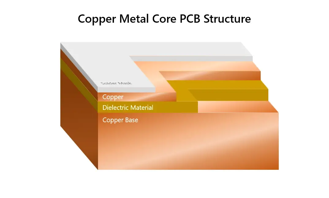
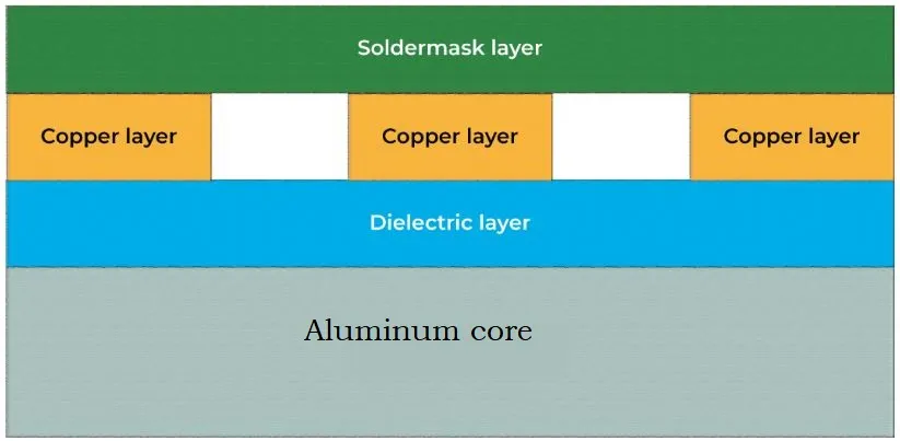
Aluminum PCBs consist of three main layers: a thick aluminum base for heat spreading, a thermally conductive dielectric layer for insulation, and a copper circuit layer on top for electrical paths. This structure allows heat from power components to transfer directly to the aluminum side, where a heatsink can be attached easily. For electronic hobbyists building LED arrays or motor controllers, these boards prevent failures caused by localized hot spots that plague ordinary PCBs. The metal core provides mechanical strength, reducing flexing during soldering or operation in vibrating environments like drone electronics. Hobbyists appreciate their dimensional stability, which maintains trace integrity even after repeated thermal cycles. Overall, aluminum PCBs enable compact designs with higher power density, making them ideal for garage workshops tackling ambitious builds.
Types of Aluminum PCBs: Single-Sided vs. Double-Sided
Single sided aluminum PCB manufacturing focuses on one copper layer atop the dielectric and aluminum base, suiting simple applications like single-sided LED strips or power resistors. This type skips complex interlayer connections, streamlining production and keeping costs low for hobbyist prototypes. Double sided aluminum PCB manufacturing adds a second copper layer, often separated by additional dielectric, allowing traces on both sides for more routing flexibility in compact power supplies. However, double-sided versions demand precise alignment during lamination to avoid shorts between layers and the core. Hobbyists choose single-sided for quick builds, while double-sided suits circuits needing ground planes on both surfaces. Both types share core fabrication steps but differ in imaging and etching complexity.
Key Materials in Aluminum PCB Manufacturing
The foundation starts with high-purity aluminum alloy sheets, typically 1 to 2 mm thick, chosen for their balance of thermal conductivity and machinability. A ceramic-filled epoxy serves as the dielectric, providing electrical isolation while allowing heat to pass through efficiently to the base. Copper foil, usually 1 to 2 ounces per square foot thick, forms the conductive traces capable of handling higher currents than thin FR4 layers. Photoresist films enable precise pattern transfer, while solder mask inks protect traces and enhance reflectivity in lighting projects. Surface finishes like organic solderability preservatives or immersion gold ensure reliable soldering without oxidation. These materials undergo rigorous cleaning before bonding to prevent defects in the final board.
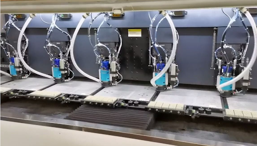
The Aluminum PCB Fabrication Process: Step-by-Step
Step 1: Material Preparation and Lamination
Factories begin by cutting aluminum sheets to panel size and cleaning them to remove oxides and contaminants. The dielectric prepreg layer bonds between the aluminum and copper foil under high heat and pressure in a lamination press, forming a solid thermal sandwich. This initial phase is the foundation of the step-by-step aluminum pcb manufacturing process, ensuring strong adhesion without voids that could trap heat. Panels are inspected for uniformity before proceeding. For double-sided boards, additional copper and dielectric layers stack symmetrically. Hobbyists note this pre-laminated stock simplifies ordering for prototypes.
Step 2: Drilling Holes
Specialized carbide drills create mounting holes or positioning vias through the copper, dielectric, and aluminum. Controlled speeds prevent cracking the brittle dielectric or burrs on the metal edges. Peck drilling cycles clear chips effectively, followed by deburring for smooth finishes. Single-sided boards need fewer holes than double-sided, which may require them for interlayer access. Plasma or chemical desmearing cleans residues from hole walls. This prepares the panel for imaging without misalignment risks.
Step 3: Circuit Pattern Imaging and Etching
Dry film photoresist laminates onto the copper surface, then UV exposure through artwork films hardens the keep-out areas. Development removes unexposed resist, revealing the circuit pattern for etching. Alkaline solutions like cupric chloride selectively dissolve excess copper, forming precise traces down to fine widths. Resist strips away chemically, leaving clean conductors. Micro-etching refines edges to prevent shorts. Double-sided manufacturing repeats this on both sides with flip alignment.
Step 4: Solder Mask and Silkscreen Application
Liquid photoimageable solder mask coats the etched board, with UV exposure defining openings over pads. Thermal curing hardens it for insulation and protection against solder bridges. White masks reflect light in LED applications, while green suits general use. Epoxy-based silkscreen ink prints legends, polarity marks, and labels via stencil. Baking ensures adhesion under thermal stress. These layers safeguard traces during handling and assembly.
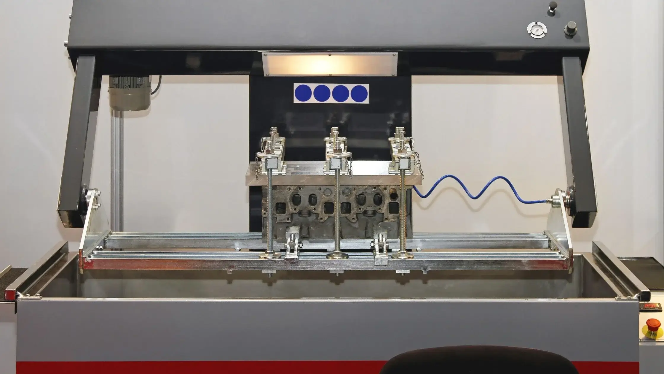
Step 5: Surface Finish, Routing, and Testing
Surface finishes apply to exposed copper for solderability and corrosion resistance. V-scoring or milling separates individual boards from panels, with tabs for fixturing during assembly. Electrical testing via flying probes checks continuity and isolation. Visual and automated optical inspections verify dimensions and defects. Thermal checks simulate operation to confirm heat paths. Packaged boards arrive ready for hobbyist soldering.
Aluminum PCB Assembly Guide
Assembly follows standard surface-mount technology but accounts for the aluminum's rapid cooling. Stencil printing deposits solder paste on pads precisely. Pick-and-place machines position components, followed by reflow ovens with profiles ramping slowly to avoid warpage from core contraction. Thermal vias under hot parts channel heat to the base effectively. Through-hole parts use selective soldering to prevent bridging. Post-reflow cleaning removes flux, with X-ray or endoscopy inspecting joints. Hobbyists attach heatsinks directly to the bare aluminum for optimal dissipation. This aluminum PCB assembly guide ensures reliable prototypes without thermal failures.
Quality Control in Metal Core PCB Manufacturing
Quality checks occur at every stage to meet IPC-A-600 acceptability criteria for hole quality and trace registration. Lamination verifies bond strength through cross-sections, preventing delamination under heat. Etching monitors undercut to maintain line widths, while solder mask alignment follows IPC-6012 specifications for pad coverage. Final electrical and thermal tests confirm performance before shipment. Automated systems reduce human error, ensuring consistency for hobbyist orders. Warpage measurements guide storage to preserve flatness.
Best Practices and Troubleshooting for Beginners
Design traces wide for high currents and place vias near heat sources to leverage the core. Specify mounting holes early to avoid redesigns. For single sided aluminum PCB manufacturing, keep layouts simple to cut costs. Test prototypes under load to validate thermal paths before scaling. Common aluminum PCB manufacturing defects include poor cleaning causing adhesion failures or mismatched reflow profiles leading to tombstoning. Consult factory capabilities for double-sided feasibility. These tips streamline your workflow from design to build.
Conclusion
Mastering the aluminum PCB fabrication process empowers hobbyists to create durable, high-performance electronics without thermal bottlenecks. From lamination to final testing, each step builds reliability into metal core PCB manufacturing. Single and double-sided options offer flexibility for diverse projects, while proper assembly maximizes heat dissipation. Adhering to quality practices ensures boards perform as expected in real-world use. Experiment confidently with these insights to push your hobby projects further.
FAQs
QX: What is the key difference in single sided aluminum PCB manufacturing versus double sided?
AX: Single sided aluminum PCB manufacturing involves one copper layer on the dielectric over aluminum, simplifying etching and reducing costs for basic heat-dissipating circuits. Double sided requires patterning both sides, adding alignment steps and plating for interlayer connections. This increases complexity but allows denser routing. Hobbyists pick single-sided for LEDs, saving time and budget. Factories handle both efficiently with precise imaging.
QX: How does the aluminum PCB fabrication process handle heat management during production?
AX: The process uses thermally conductive dielectrics laminated to aluminum cores, ensuring heat paths form early. Drilling and etching preserve these paths without compromising insulation. Solder mask and testing verify dissipation under simulated loads. This prevents defects like voids from thermal expansion mismatches. Beginners benefit from specifying high-conductivity materials upfront.
QX: What should beginners know about the aluminum PCB assembly guide for prototypes?
AX: Start with solder paste stenciling, then reflow with adjusted profiles to match aluminum cooling rates, avoiding warpage. Use thermal pads or vias for components like power transistors. Inspect joints visually and test functionality. This guide minimizes rework in hobby workshops. Double-check heatsink mounting for full performance.
QX: Why reference standards in metal core PCB manufacturing?
AX: Standards like IPC-A-600 guide acceptability of traces and holes, ensuring reliable boards. They standardize quality across factories for consistent hobbyist results. Following them reduces failures in high-heat applications. This factory-driven approach builds confidence in prototypes.
References
- IPC-A-600K — Acceptability of Printed Boards. IPC, 2020
- IPC-6012E — Qualification and Performance Specification for Rigid Printed Boards. IPC, 2017
- J-STD-001H — Requirements for Soldered Electrical and Electronic Assemblies. IPC, 2018