Introduction
Power electronics applications, such as inverters, converters, and motor controllers, often require PCBs that handle substantial currents while maintaining reliability under thermal stress. Standard PCBs with 1 oz copper thickness on outer layers suffice for many designs, but high-power scenarios demand thicker copper to enhance PCB current carrying capacity. High outer layer copper thickness PCBs, typically featuring 2 oz or greater on external layers, address these needs by supporting high current PCB design without excessive trace widths. This approach reduces overall board size and improves efficiency in compact systems. Engineers must understand the implications of heavy copper implementation to balance performance and manufacturability. Factory processes adapt specifically for these boards to ensure quality and adherence to industry benchmarks.
Defining High Outer Layer Copper Thickness PCBs and Their Relevance
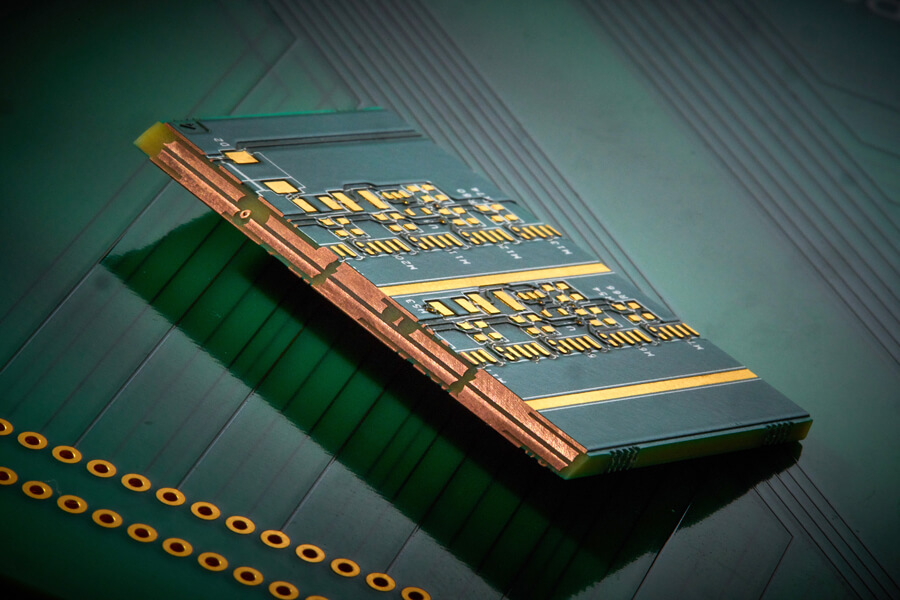
High outer layer copper thickness PCBs refer to boards where the external copper layers exceed standard weights, often reaching 3 oz/ft2 (105 μm) or more, while inner layers may remain thinner for signal integrity. This configuration is prevalent in power electronics PCB designs, where asymmetric copper distribution optimizes outer layer performance for current handling. The primary relevance lies in elevating PCB current carrying capacity, allowing traces to manage tens of amperes with controlled temperature rise. Thick copper PCB benefits include superior heat dissipation, as thicker foils act as efficient thermal conduits to the environment. In high-power applications, this prevents hotspots and extends component life. Manufacturers prioritize these boards for sectors like renewable energy systems and industrial drives, where reliability under load is paramount.
Technical Principles Behind Enhanced Performance
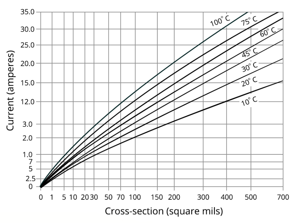
The core principle governing these PCBs is the relationship between copper cross-section, current density, and thermal rise, as outlined in IPC-2152. Thicker outer copper increases the conductor's cross-sectional area, directly boosting ampacity while minimizing voltage drop over distance. For instance, external traces benefit from natural convection cooling, making outer layer thickening particularly effective for high current paths. Heat generated by I2R losses dissipates faster through bulkier copper, coupling well with vias or heat sinks. Engineers calculate trace requirements using IPC-2152 nomographs, factoring in ambient temperature, layer position, and copper weight. This standard supersedes older models by incorporating real-world test data, ensuring conservative designs for safety.
Inner layers often stay at 1–2 oz to preserve dielectric spacing and impedance control, creating an asymmetric build-up that influences board mechanics. Thermal expansion mismatches between copper and substrate amplify under high currents, but proper material selection mitigates risks. Power electronics PCB layouts leverage outer heavy copper for bus bars or power planes, distributing current evenly. Simulations validate these principles, predicting hotspots before fabrication. Overall, the physics favor outer thickening for exposed-layer advantages in convection-dominated cooling.
PCB Current Carrying Capacity: Calculations and Considerations
Determining PCB current carrying capacity starts with defining allowable temperature rise, typically 20–30°C above ambient for reliability. IPC-2152 provides charts differentiating external and internal traces, showing how 4 oz outer copper might halve required widths compared to 1 oz for the same current. External layers excel due to air cooling, while internals rely on conduction through dielectrics. High current PCB design thus prioritizes outer thickness for primary power paths, using wider traces or planes where needed. Vias in series with traces add resistance, so filled or plated-through vias enhance capacity in multilayer stacks.
Factors like board population density and enclosure airflow further refine calculations. Designers adjust for these via derating factors in IPC-2152. Heavy copper reduces the need for parallel traces, simplifying routing in dense boards. However, overestimation risks underutilization, while conservatism ensures margins. Integrating thermal vias or embedded heat pipes complements copper benefits in extreme cases.
Thick Copper PCB Benefits in High-Power Scenarios
Thick copper PCB benefits extend beyond mere ampacity to mechanical robustness and space efficiency. Heavier outer layers provide structural reinforcement, resisting flexing in vibration-prone environments like automotive power modules. Enhanced thermal management lowers junction temperatures of attached power devices, improving MTBF. In power electronics PCB applications, this translates to fewer failures from electromigration or solder joint fatigue. Manufacturing yields compact designs, as narrower traces free real estate for controls or passives. Cost savings arise from reduced layer count in some hybrids.
Another advantage is better electromagnetic compatibility, with thicker copper lowering inductance in power loops. This aids compliance in high di/dt scenarios. Long-term, these boards support higher power densities, aligning with trends in electrification. Engineers report fewer redesigns when starting with heavy copper foresight.
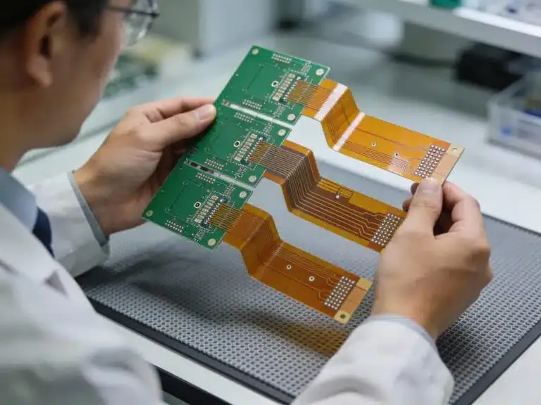
Heavy Copper PCB Manufacturing: Processes and Challenges
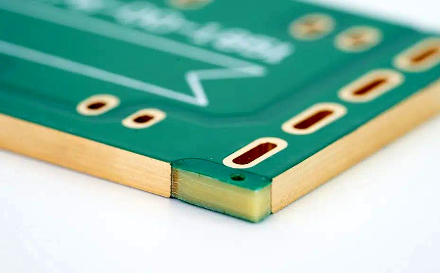
Heavy copper PCB manufacturing demands specialized techniques, starting with panel preparation using high-grade copper-clad laminates. Outer layers undergo extended electroplating to build thickness, often panel plating followed by pattern plating for fine features. This process, lasting hours, ensures uniform deposition but risks uneven buildup if current density varies. Etching presents challenges, as thicker foils require tented or differential methods to prevent undercuts and sidewall roughness. Adherence to IPC-6012 ensures minimum copper thickness post-etch, critical for performance.
Warpage emerges as a key issue due to asymmetric copper weights, exacerbated during lamination and reflow. Manufacturers counter this with balanced inner copper pours, carrier panels, or sequential lamination. Drilling larger vias for heavy copper demands precise control to avoid breakout. Solder mask application adapts with thicker formulations to cover tall traces without voids. Final fabrication includes beveling edges for assembly fit. Quality checks verify wrap plating thickness per IPC-6012 criteria.
Warpage mitigation involves CTE-matched materials and controlled curing. Post-etch inspections confirm trace integrity, rejecting boards with excessive pitting.
High Current PCB Design Best Practices
Effective high current PCB design begins with early specification of copper weights in stackups. Allocate outer layers for power, reserving inners for signals to minimize crosstalk. Route power traces straight, minimizing bends to reduce resistance. Incorporate thermal reliefs on pads for soldering, avoiding full copper pours that trap heat. Via stitching along edges distributes current and aids cooling.
Layer sequencing places heavy copper outermost, with ground planes adjacent for return paths. Simulate power integrity using field solvers tied to IPC-2152 data. Prototype testing validates models, measuring actual temp rise under load. Collaboration with fabricators ensures DFM compliance from Gerber release.
Applications in Power Electronics
In power electronics PCB realms, these boards power DC-DC converters handling kilowatts. Motor drives benefit from compact heavy copper planes feeding IGBTs. Welding equipment and UPS systems leverage the durability for pulsed loads. Renewable inverters use them for grid-tie efficiency. Each application underscores the synergy of thick copper with silicon carbide devices demanding low loss paths.
Conclusion
High outer layer copper thickness PCBs elevate high current PCB design by amplifying PCB current carrying capacity and thermal resilience. Thick copper PCB benefits, from space savings to reliability gains, justify manufacturing adaptations despite challenges like warpage. Adhering to standards like IPC-2152 and IPC-6012 ensures predictable outcomes. Engineers gain a powerful tool for power electronics PCB innovation, balancing performance with practicality. Future designs will increasingly rely on these robust solutions as power demands escalate.
FAQs
Q1: What factors most influence PCB current carrying capacity in heavy copper designs?
A1: PCB current carrying capacity depends on copper thickness, trace width, temperature rise allowance, and layer position, as detailed in IPC-2152 charts. External outer layers with thick copper excel due to convection cooling, allowing higher currents than internals. Designers must account for ambient conditions and board density for accurate sizing. This approach optimizes high current PCB design reliability.
Q2: Why choose thick copper PCB benefits for power electronics PCB applications?
A2: Thick copper PCB benefits include superior heat dissipation, higher ampacity per trace area, and mechanical strength, ideal for power electronics PCB handling tens of amperes. Narrower traces save space while managing thermal loads effectively. These advantages reduce system size and enhance longevity in demanding environments like inverters.
Q3: What are common challenges in heavy copper PCB manufacturing?
A3: Heavy copper PCB manufacturing faces extended plating times, etching undercuts, and warpage from asymmetry. Solutions involve differential etching, balanced copper distribution, and precise lamination controls. Standards like IPC-6012 guide thickness verification post-process. Early DFM reviews prevent issues in high current designs.
Q4: How does high outer layer copper improve high current PCB design?
A4: High outer layer copper thickness boosts cross-section for better current handling and cooling, per IPC-2152 guidelines. It enables compact layouts in power paths, minimizing voltage drops. Combined with proper via design, it supports robust high current PCB design for electronics.
References
IPC-2152 — Standard for Determining Current-Carrying Capacity in Printed Board Design. IPC, 2009
IPC-6012E — Qualification and Performance Specification for Rigid Printed Boards. IPC, 2015
IPC-2221 — Generic Standard on Printed Board Design. IPC, 2009