Introduction
Electrical engineers often select 1 oz copper for its optimal balance between electrical performance, cost, and manufacturability in PCB designs. With a nominal thickness of 35 microns, 1 oz copper supports reliable current carrying capacity up to several amps per trace while allowing finer feature sizes compared to heavier weights like 2 oz. As designs evolve toward higher densities, advanced PCB design 1 oz copper techniques become essential to achieve compact layouts without sacrificing signal integrity or reliability. This article delves into strategies for high-density PCB design using 1 oz copper, including HDI PCB 1 oz copper structures, microvias 1 oz copper integration, and accommodations for fine-pitch components 1 oz copper. Engineers can leverage these methods to meet stringent space constraints in applications such as telecommunications, computing, and automotive electronics. Mastering these approaches requires a deep understanding of material interactions and process capabilities.
Why 1 oz Copper Excels in Advanced High-Density Designs
1 oz copper provides sufficient conductivity for most high-speed signals while enabling tighter trace widths and spaces essential for high-density PCB design. Thicker copper weights increase etching undercuts, complicating fine-line production, but 1 oz maintains consistent sidewall profiles during standard subtractive etching processes. In HDI environments, this thickness supports microvia formation without excessive plating buildup that could hinder laser drilling accuracy. Its prevalence stems from alignment with IPC Class 2 and Class 3 requirements, ensuring broad fabricator compatibility. Furthermore, 1 oz copper facilitates controlled impedance stackups by pairing well with low-loss dielectrics, critical for maintaining signal quality at gigabit speeds. Designers prioritize it to avoid the premium costs and handling complexities of ultrathin foils under 1/2 oz.
Core Technical Principles for 1 oz Copper in HDI Structures
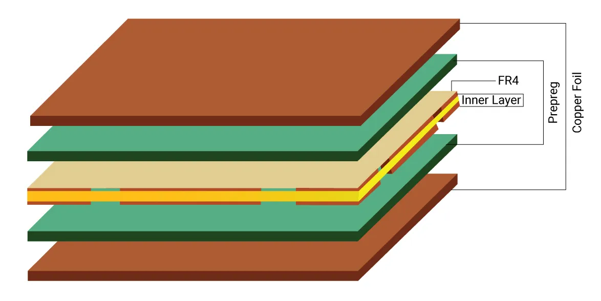
Advanced designs with 1 oz copper rely on precise stackup planning to optimize layer count and via transitions. Microvias, defined by IPC-2226 as blind or buried vias with aspect ratios up to 1:1, connect outer layers to inner planes effectively when using 1 oz copper on buildup layers. The copper weight influences via reliability, as plating thickness must fill the barrel uniformly without voids, adhering to IPC-6012 performance specifications for rigid boards. Signal propagation benefits from reduced skin effect losses at frequencies below 10 GHz compared to thicker copper. Thermal expansion matching between 1 oz copper and core materials minimizes stress during reflow, preserving via integrity. Engineers calculate trace dimensions using standard formulas, ensuring widths of 4-6 mils support 100-ohm differential pairs in typical 100-micron dielectric separations.
High-density routing demands adherence to minimum spacing rules scaled to copper weight. For 1 oz copper, fabricators achieve 3/3 mil (line/space) in production, enabling escape routing from fine-pitch arrays. Impedance control involves iterative field solver adjustments, accounting for copper roughness that adds 5-10% to effective dielectric constant. Power distribution networks benefit from solid 1 oz planes segmented to reduce inductance. Via staggering in microvia stacks prevents alignment issues during sequential lamination. These principles form the foundation for robust HDI PCB 1 oz copper performance.
Implementing Microvias with 1 oz Copper: Design and Reliability
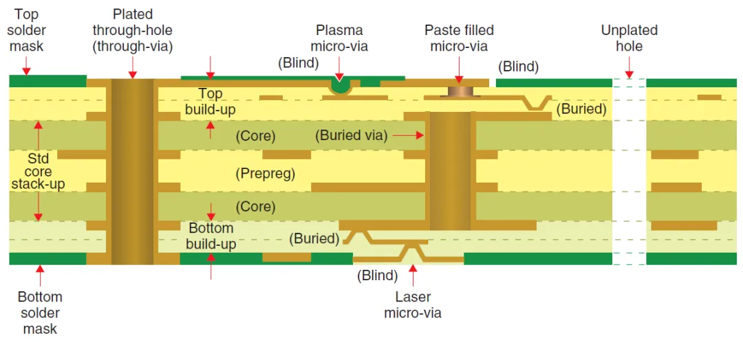
Microvias 1 oz copper integration starts with laser ablation on buildup foils, where 1 oz thickness allows clean dielectric removal without copper smearing. Post-drilling, electroless and electrolytic plating deposits 15-20 microns to fill vias, ensuring low resistance paths under IPC-6012 criteria. Stacked microvias, common in Type III HDI, require offset placement to avoid drill wander, with pad sizes minimized to 75 microns for density gains. Reliability testing focuses on thermal cycling, as 1 oz copper's ductility resists cracking better than thinner foils under CTE mismatch. Designers incorporate filled vias for planar surfaces, aiding fine-pitch component mounting. Aspect ratios below 0.8:1 guarantee plating uniformity, preventing electromigration in high-current paths.
Challenges arise from copper etchback during sequential processing, so specifying photoresist adhesion promoters enhances definition. Electrical testing verifies continuity post-lamination, targeting less than 50 mOhm per via. For high-layer counts, hybrid stacks combine mechanical through-vias with laser microvias on 1 oz outer layers. This approach maximizes interconnect density while controlling cost. Simulation tools predict thermal-mechanical stress, guiding via capture pad enlargement to 50% of drill diameter.
Routing Strategies for Fine-Pitch Components on 1 oz Copper
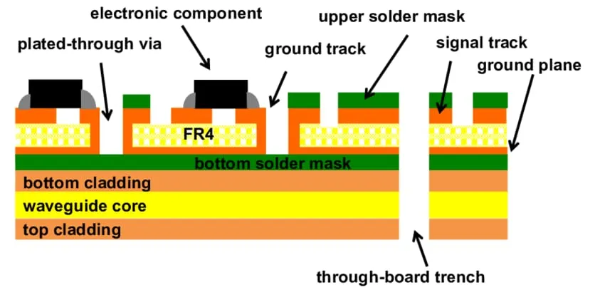
Fine-pitch components 1 oz copper, such as 0.4 mm pitch BGAs, demand fanout routing with microvias directly under pads. Traces narrower than 4 mils escape the perimeter, fanning out to wider lines for signal distribution. Differential pairs maintain 90-100 ohm impedance by adjusting separation to 5-6 mils in 1 oz copper. Length tuning compensates skew, using serpentine patterns confined to inner layers to minimize crosstalk. Power and ground vias interleave with signal escapes, forming low-inductance returns. Dogbone vias connect BGA pads to microvias, optimizing space in high-density PCB design.
Component shadowing limits routing layers, so prioritize critical nets on outer 1 oz layers for accessibility. Solder mask defined pads with 75% enlargement prevent bridging during assembly. For QFN packages, exposed pads route through thermal vias filled with conductive epoxy, dissipating heat via inner planes. These techniques enable over 1000 I/Os per square inch without heroic measures. Verification involves DRC checks against fabricator DFM rules, ensuring annular rings exceed 20% of drill size.
Power Integrity and Thermal Management in Dense 1 oz Copper Layouts
Power delivery in advanced PCB design 1 oz copper uses decoupled planes with cutouts for decoupling caps near ICs. 1 oz copper supports current densities up to 1.5 A/mm width at 10°C rise, suitable for digital logic. Thermal vias arrays under hot components conduct heat to inner 1 oz planes, spaced at 0.5 mm grids. Stackups with 1 oz power planes sandwich thin dielectrics to lower plane resonance. Decoupling strategies place 0.1 uF caps within 1 mm of pins, minimizing loop inductance. Simulations predict PDN impedance below 10 mOhm up to 1 GHz.
Thermal reliefs on vias prevent solder wicking while allowing heat flow. For high-power apps, widen traces to 20 mils or pour copper polygons. These practices align with JEDEC guidelines for thermal characterization, ensuring junction temperatures stay under limits.
Best Practices and DFM Considerations
Stackup symmetry prevents warpage, with 1 oz copper balanced across layers. Specify sequential lamination for HDI buildup, verifying via fill via cross-sectioning. Route high-speed signals away from edges to avoid fringing fields. Incorporate test points on 1 oz traces for in-circuit verification. Collaborate with fabricators early on capabilities like 3 mil features. Final Gerber reviews catch spacing violations before production.
Troubleshooting Common Issues in 1 oz Copper HDI Designs
Warpage from asymmetric stacks manifests as bow over 0.75%, correctable by core selection per IPC standards. Signal attenuation in long 1 oz traces requires equalizer insertion or thicker inner layers. Via opens trace to plating shorts, resolved by aspect ratio control. Fine-pitch solder balls stem from mask misalignment, fixed by NSMD pads. Systematic DFM audits mitigate these, ensuring first-pass yield.
Conclusion
Advanced PCB design 1 oz copper unlocks high-density PCB design potential through optimized microvias 1 oz copper, fine-pitch components 1 oz copper handling, and robust stackups. Engineers achieve superior performance by integrating IPC-guided principles for vias, routing, and integrity. These techniques balance density, reliability, and cost for next-generation electronics. Prioritizing simulation and DFM elevates designs from viable to exceptional.
FAQs
Q1: Can microvias 1 oz copper support HDI PCB 1 oz copper in 12-layer stacks?
A1: Yes, microvias 1 oz copper enable Type III HDI structures per IPC-2226 guidelines, with stacked configurations connecting multiple layers. Aspect ratios under 0.8:1 ensure reliable plating, while offset placement avoids drill breakthrough. Electrical engineers verify integrity through thermal cycling tests, achieving densities over 150,000 vias per square meter. This approach suits compact telecom modules without excessive cost.
Q2: What trace dimensions work best for high-density PCB design with 1 oz copper?
A2: In high-density PCB design, 1 oz copper supports 3-4 mil traces and spaces for Class 3 boards, enabling fine-pitch escapes. Impedance calculators adjust widths for 50/100 ohm targets in 100-micron dielectrics. Fabricator capabilities dictate limits, typically 3/3 mil minimum. Logical stackup planning pairs this with microvias for optimal routing density.
Q3: How does 1 oz copper handle fine-pitch components 1 oz copper in advanced designs?
A3: Fine-pitch components 1 oz copper like 0.35 mm BGAs route via dogbone microvias on 1 oz layers, fanning out to 5 mil traces. NSMD pads with 75 micron capture ensure assembly reliability. Power/ground interleaving reduces inductance. Engineers simulate crosstalk to confirm signal quality at multi-Gbps rates.
Q4: Are there thermal limits for advanced PCB design 1 oz copper in power-heavy apps?
A4: 1 oz copper manages 1-2 A per 10 mil trace at 20°C rise, per standard calculators. Thermal vias and plane pours dissipate heat effectively in HDI stacks. JEDEC thermal models predict hotspots, guiding via arrays. Balanced designs keep components under spec without heavier copper.
References
IPC-2226 - Sectional Design Standard for High Density Interconnect (HDI) Printed Boards. IPC.
IPC-6012D - Qualification and Performance Specification for Rigid Printed Boards. IPC.
IPC-6016 - Qualification and Performance Specification for High Density Interconnect (HDI) Printed Boards. IPC.