Introduction
Printed circuit boards traditionally feature rectangular outlines for efficient production workflows. However, modern designs often require irregular PCB shapes to fit unique enclosures or optimize space in compact devices. These non-standard contours introduce complexities that directly influence PCB shape manufacturing cost. Engineers must balance aesthetic and functional demands with fabrication pricing factors to avoid unexpected expenses. Understanding these impacts enables better PCB design for manufacturing from the outset. This article explores how odd shapes affect costs across key processes.
Defining Irregular PCB Shapes and Their Relevance
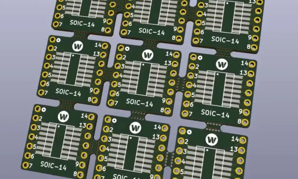
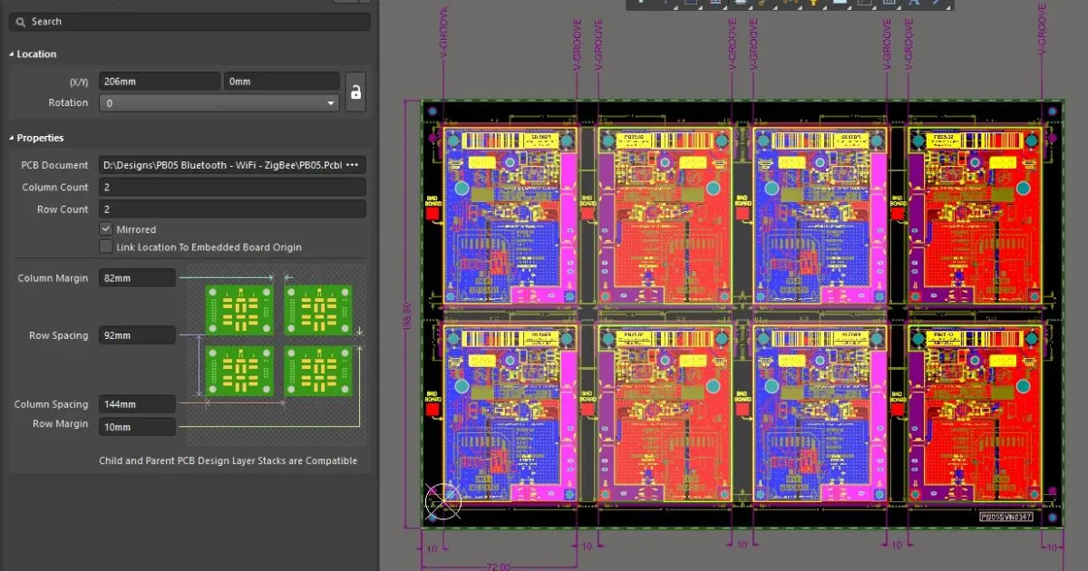
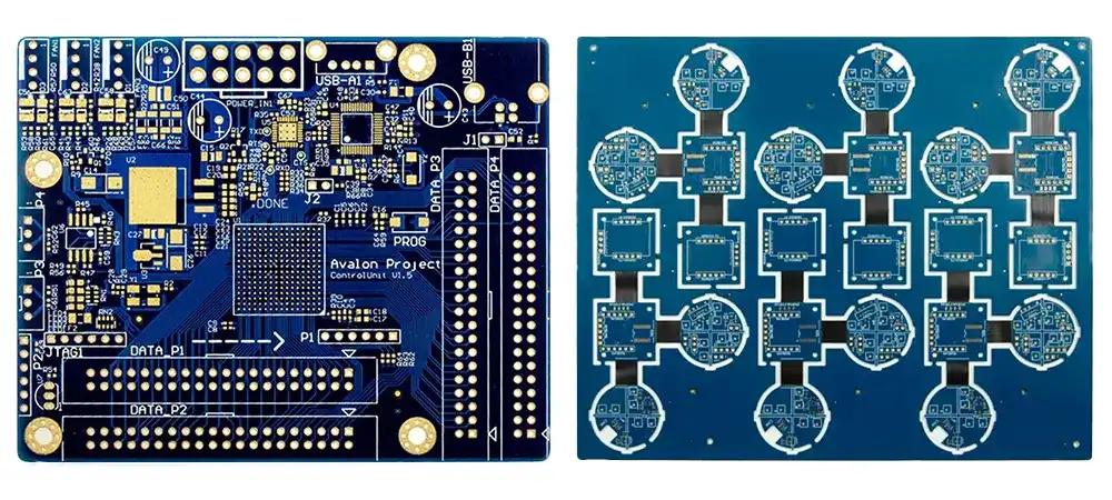
Irregular PCB shapes deviate from standard rectangular or simple polygonal forms, including curves, cutouts, or asymmetrical profiles tailored to product housings. Such designs arise in applications like wearables, automotive modules, or medical devices where form factor dictates performance. The irregular PCB shape cost stems primarily from reduced efficiency in material use and processing. Rectangular boards align seamlessly with production panels, maximizing yield per sheet. In contrast, odd contours demand custom nesting algorithms during panelization, often leaving more scrap material. This inefficiency compounds as production scales, making shape a critical PCB fabrication pricing factor.
Factory insights reveal that while rectangular boards achieve near 90 percent panel utilization in standard runs, irregular shapes frequently drop below 70 percent depending on complexity. Engineers evaluating prototypes overlook this until quoting production volumes. Adhering to design guidelines early mitigates these hikes. Relevance grows with miniaturization trends, where every millimeter of board real estate influences overall system costs.
Mechanisms Driving Cost Increases in Fabrication
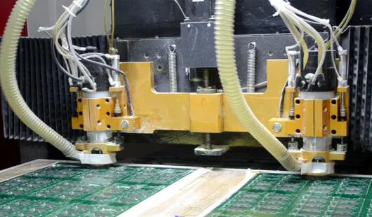
Panelization represents the first major cost driver for irregular shapes. Manufacturers array multiple boards on large substrate sheets to minimize waste, but odd profiles resist tight packing. Complex algorithms or manual adjustments extend preparation time, and suboptimal layouts increase raw material consumption. For instance, curved edges create gaps that rectangular boards avoid, directly elevating per-unit expenses.
Routing and contour milling amplify these issues. Standard rectangular boards use V-scoring or simple tabbing for depanelization, which is fast and low-wear on tools. Irregular contours require prolonged CNC milling with specialized bits to achieve precise outlines. Tool changes mid-job and higher bit consumption add to overhead. IPC-6012E specifies tolerances for board outlines, typically plus or minus 0.15 mm for Class 2 boards, demanding meticulous control to prevent defects like overcuts or burrs.
Warpage control poses another challenge. Thin, irregularly shaped boards experience uneven stress during lamination and etching, exacerbating bow and twist beyond rectangular norms. This necessitates custom baking or fixturing, per IPC-6012E requirements for planar integrity. Additional metrology steps, such as dial gauge measurements, verify compliance but extend cycle times. These factors collectively raise PCB fabrication pricing factors by 20 to 50 percent for highly contoured designs, based on process engineering observations.
Assembly and Testing Complications from Odd Shapes
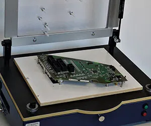
Assembly processes face heightened fixturing demands with irregular PCB shapes. Pick-and-place machines rely on fiducials and edge support, but asymmetrical profiles risk misalignment or vibration. Custom pallets or vacuum fixtures become essential, incurring design and fabrication costs not needed for squares. Solder paste application via stencils also suffers if shapes prevent uniform tensioning.
Testing amplifies expenses further. In-circuit and flying probe testers require tailored bed-of-nails or probe layouts to access all nets without board flex. Irregular edges complicate secure clamping, potentially mandating soft-touch adapters. J-STD-001G guidelines for soldering and handling underscore the need for stable support to avoid defects like tombstoning on contoured peripheries. These adaptations shift labor from high-volume throughput to bespoke setups.
Yield losses compound across stages. Handling irregular boards increases drop risks during transport between lines, while depaneling stress can propagate microcracks. Engineers optimizing for cost prioritize shapes that align with standard tooling envelopes.
Best Practices for Cost-Optimized PCB Shapes
Start with design for manufacturing principles to curb irregular PCB shape cost. Use IPC-2221 generic requirements to evaluate outline feasibility early, favoring gentle curves over sharp indents that demand small-radius tools. Simulate panelization in layout software to target over 80 percent utilization, adjusting component placement accordingly.
Simplify contours where possible. Replace complex arcs with faceted approximations using minimum radius guidelines, typically 0.5 mm for routing efficiency. Incorporate breakaway tabs or mouse bites for depanelization, reducing full milling needs. Collaborate with fabrication partners on Gerber reviews to refine nesting before tape-out.
For assembly, position fiducials symmetrically and avoid edges nearer than 5 mm to contours. Select materials with matched CTE to minimize warpage in thin, odd boards. Prototype small runs to validate yields before scaling. These steps integrate PCB design for manufacturing seamlessly, often halving premiums over fully custom shapes.
Real-World Insights from Manufacturing Floors
Factory data highlights patterns in cost variances. Rectangular boards in 18 by 24 inch panels yield uniformly, while a single irregular design might halve effective output per sheet. Troubleshooting reveals that 40 percent of odd-shape rejects trace to routing tolerances or handling slips. Engineers iterating on prototypes learn to bound complexity with bounding boxes for partial standardization.
One common pitfall involves multilayer stacks with internal cutouts, where alignment drifts amplify during lamination. Preemptive stackup reviews per IPC standards prevent this. Scaling from prototype to production exposes these gaps, underscoring early DFM.
Conclusion
Irregular PCB shapes offer design freedom but elevate costs through inefficient panelization, extended routing, custom fixturing, and yield risks. Key PCB fabrication pricing factors like material waste and process time dominate the equation. By embracing cost-optimized PCB shapes and PCB design for manufacturing practices, engineers achieve balance. Reference standards like IPC-6012E ensure compliance without excess. Prioritizing these insights streamlines production and preserves budgets.
FAQs
Q1: How does irregular PCB shape cost compare to standard rectangular boards?
A1: Irregular shapes increase costs mainly via poor panel utilization and complex routing, often adding 20 to 50 percent to base pricing depending on contour intricacy. Rectangular boards maximize material efficiency and use standard tools. To minimize, simulate nesting early in design. Factory workflows favor shapes fitting common panel grids for optimal PCB shape manufacturing cost control.
Q2: What are the top PCB fabrication pricing factors tied to board shape?
A2: Panelization yield, CNC milling time, and fixturing needs top the list for non-standard shapes. Odd profiles waste substrate and wear tools faster than rectangles. Tolerances per IPC-6012E demand precision, extending inspection. Engineers mitigate by simplifying outlines and using tabs, directly impacting overall expenses.
Q3: How can engineers achieve cost-optimized PCB shapes?
A3: Favor faceted curves over smooth arcs and align with panel dimensions during layout. Incorporate standard depanelization like V-scoring where feasible. Validate via DFM checks referencing IPC-2221 for feasibility. This approach boosts yield and cuts custom tooling, essential for PCB design for manufacturing.
Q4: Why do irregular shapes affect assembly more than fabrication?
A4: Assembly requires bespoke pallets for stability, unlike fabrication's focus on material. Misalignment risks rise with asymmetry, per J-STD-001G handling rules. Custom stencils and testers add setup time. Rectangular forms leverage universal jigs, streamlining throughput.
References
IPC-6012E — Qualification and Performance Specification for Rigid Printed Boards. IPC, 2017
IPC-2221B — Generic Standard on Printed Board Design. IPC, 2012
J-STD-001G — Requirements for Soldered Electrical and Electronic Assemblies. IPC, 2017