Introduction
Heavy copper PCBs represent a critical advancement in printed circuit board technology, particularly for applications demanding high performance under demanding conditions. These boards feature copper layers significantly thicker than standard 1 oz per square foot, typically starting from 3 oz per square foot or more, which translates to thicknesses exceeding 105 microns. This construction delivers substantial improvements in heavy copper PCB reliability, making them indispensable for power electronics, automotive systems, and industrial controls where failures can lead to costly downtime. Engineers often select heavy copper PCBs to handle elevated currents without excessive heating, thereby reducing risks associated with thermal stress and mechanical wear. Factory processes for these boards emphasize precise plating and etching to maintain integrity across multiple layers. Ultimately, adopting heavy copper PCBs enhances overall system durability and extends operational lifetime in environments prone to vibration and temperature fluctuations.
What Are Heavy Copper PCBs and Why Do They Matter?
Heavy copper PCBs are defined by their copper foil weights ranging from 3 oz/ft2 to 20 oz/ft2 or higher on one or more layers, contrasting with conventional boards limited to 1 or 2 oz/ft2. This increased thickness allows for wider traces and planes capable of carrying higher currents with minimal resistance, a key factor in heavy copper PCB durability. In manufacturing, heavy copper boards require specialized techniques such as differential etching and extended plating cycles to achieve uniform thickness without defects. These boards matter in high-reliability sectors because standard PCBs often fail under sustained high loads, leading to overheating or trace fractures. For electrical engineers designing power supplies or inverters, heavy copper construction aligns with the need for robust performance metrics outlined in industry standards like IPC-6012E. By prioritizing these boards, designers ensure compliance with qualification tests for rigid printed boards, fostering confidence in long-term deployment.
The relevance extends to thermal management challenges prevalent in modern electronics. Thicker copper facilitates efficient heat spreading, directly addressing heavy copper PCB thermal stress concerns during operation or assembly reflow. Factories producing these boards focus on laminate selection and lamination pressures to prevent delamination under thermal cycling. This approach not only boosts heavy copper PCB lifetime but also simplifies board sizing by enabling fewer layers for the same power density. Engineers benefit from reduced design iterations when incorporating heavy copper early, as it preempts common failure modes observed in lighter constructions.
Technical Mechanisms Driving Heavy Copper PCB Reliability
The core mechanism behind heavy copper PCB reliability lies in the reduced electrical resistance provided by thicker copper cross-sections. According to design guidelines in IPC-2221, trace widths and thicknesses must balance current capacity with allowable temperature rise, where heavy copper excels by minimizing I2R losses. This results in lower voltage drops across conductors, preserving signal integrity in power distribution networks. Furthermore, the enhanced cross-sectional area distributes current more evenly, preventing localized hotspots that degrade insulation over time. Manufacturing insights reveal that precise control during copper plating ensures void-free deposits, critical for sustained performance.
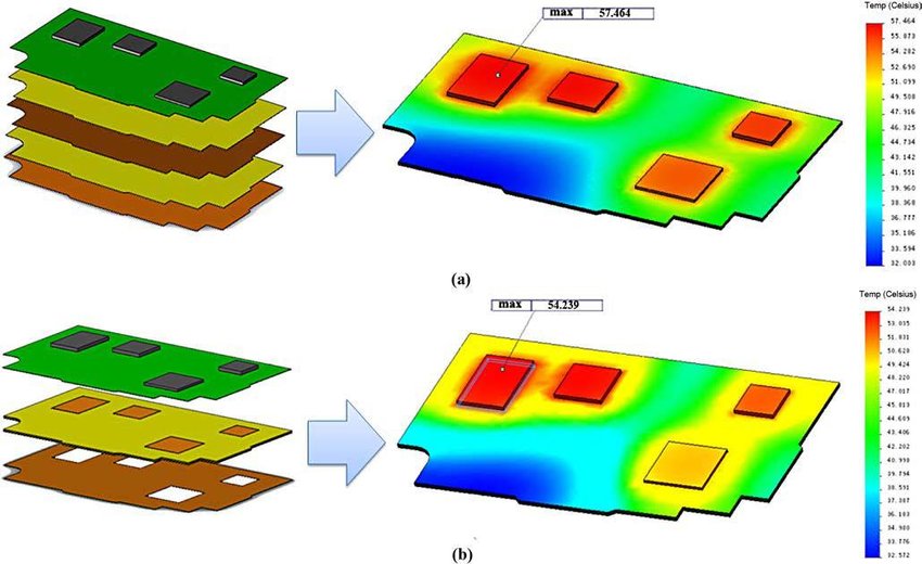
Thermal dissipation forms another pillar of reliability. Heavy copper's superior thermal conductivity, approximately 400 W/m·K, allows rapid heat transfer away from components, mitigating heavy copper PCB thermal stress during high-power operation. In multilayer stacks, thick planes act as heat spreaders, equalizing temperatures across the board and reducing gradients that cause warping. Factory-driven processes, such as step plating for vias, reinforce plated-through-hole integrity against thermal expansion mismatches. Studies on thermal cycling demonstrate that boards with 2 oz/ft2 or thicker plating in holes exhibit near-zero failure rates after multiple cycles, underscoring their robustness.
Mechanical strength further elevates heavy copper PCB durability. The increased copper volume resists flexing and vibration better than thin foils, as the stiffness scales with thickness cubed. This property proves vital in applications like motor drives, where repeated mechanical loads accompany thermal excursions. During fabrication, heavy copper boards undergo rigorous acceptability checks per IPC-A-600K to verify no cracks or lifts occur post-etching. Overall, these mechanisms interconnect to deliver a board that withstands combined electrical, thermal, and physical stresses far beyond standard limits.
Mitigating Thermal Stress in Heavy Copper PCBs
Heavy copper PCB thermal stress arises primarily from coefficient of thermal expansion differences between copper and the dielectric substrate during heating and cooling. Thicker copper layers buffer these effects by providing a more compliant interface, distributing strains evenly and preventing microcracks in vias or traces. In power applications, where components generate substantial Joule heating, heavy copper planes efficiently conduct heat to sinks or the ambient, maintaining junction temperatures within safe limits. Factory lamination uses controlled pressure profiles to bond thick foils without voids, ensuring consistent thermal paths throughout the stackup.
Effective via design plays a pivotal role in thermal relief. Plated-through vias with heavy copper barrel plating, often exceeding 50 microns, bridge layers for vertical heat flow while enduring cyclic expansion. This configuration aligns with performance specifications that demand low thermal resistance in high-density interconnects. Engineers observe that such vias reduce peak stresses by up to significant margins compared to minimal plating, directly contributing to heavy copper PCB reliability. Post-fabrication, boards undergo thermal shock testing to validate stress mitigation before shipment.
Improving Durability and Mechanical Integrity
Heavy copper PCB durability stems from the inherent toughness of thicker conductors against environmental aggressors. Vibration and shock, common in automotive or aerospace uses, induce fatigue in thin traces, but heavy copper's mass dampens resonances and resists fracture propagation. Manufacturing employs high-Tg laminates paired with thick copper to minimize warpage during soldering, a frequent durability concern. Sequential lamination builds multilayers without compromising flatness, allowing reliable component mounting.
Plated features benefit immensely from heavy copper. Hole walls plated to 2 oz/ft2 equivalent withstand barrel cracking from thermal-mechanical fatigue, as evidenced in cycling tests. This durability extends board lifetime by preserving electrical continuity under repeated flexure. Factories prioritize etch factor control to maintain sidewall integrity, avoiding undercuts that weaken mechanical bonds.
Extending Heavy Copper PCB Lifetime
Heavy copper PCB lifetime surpasses standard boards through cumulative reductions in failure drivers. Lower operating temperatures from efficient dissipation slow aging mechanisms like electromigration and intermetallic growth in solder joints. In high-current scenarios, this translates to thousands of additional hours before degradation thresholds. Reliability models incorporate these factors, predicting MTBF extensions based on derated stress levels.
Combined stressors see synergistic improvements. Thermal cycling paired with humidity challenges thin boards via conductive anodic filamentation, but heavy copper's barrier effect and robust plating inhibit ingress. Field insights from industrial deployments confirm fewer returns for heavy copper designs. By adhering to qualification protocols, manufacturers guarantee lifetimes aligned with mission profiles.
Best Practices for Design and Manufacturing of Heavy Copper PCBs
Designers should calculate trace dimensions using IPC-2221 formulas, scaling widths for heavy copper to optimize fill factor while respecting routing constraints. Asymmetric stackups demand balanced copper distribution to avert bow and twist. Thermal vias arrays under hot components channel heat effectively, sized for plating uniformity.
In manufacturing, differential etching speed handles thick foils, preventing over-etch on inner layers. Step-down plating builds vias progressively, ensuring 1:1 aspect ratios. Post-plate annealing relieves residual stresses, enhancing heavy copper PCB reliability. Incoming inspections verify foil adhesion per peel strength tests.
Assembly considerations include reflow profiles adjusted for thermal mass. Larger solder volumes accommodate pad strength from thick copper. These practices, rooted in factory expertise, yield boards ready for demanding service.
Conclusion
Heavy copper PCBs fundamentally boost reliability by excelling in current handling, thermal stress resistance, durability, and lifetime extension. Electrical engineers gain from their factory-proven construction, aligned with key standards for qualification and design. Integrating these boards streamlines high-power projects, minimizing risks and enhancing performance. Future designs will leverage even thicker variants as power densities rise, solidifying their role in reliable electronics.
FAQs
Q1: What factors contribute most to heavy copper PCB reliability?
A1: Heavy copper PCB reliability arises from thicker layers that reduce resistance, improve heat spreading, and strengthen mechanical bonds. These attributes lower failure risks in thermal cycling and high-current operation. Factory processes ensure uniform plating, vital for consistent performance. Standards like IPC-6012E guide qualification to verify these benefits.
Q2: How does heavy copper improve PCB durability under mechanical stress?
A2: Heavy copper PCB durability enhances through increased stiffness and vibration damping from thick traces and planes. This resists fatigue cracking in dynamic environments like automotive systems. Thicker plating in vias bolsters hole wall integrity. Manufacturing focuses on warp control for reliable assembly.
Q3: Why is thermal stress management critical for heavy copper PCBs?
A3: Heavy copper PCB thermal stress management prevents hotspots and delamination via superior conductivity and strain distribution. Thicker copper equalizes temperatures, protecting components during peaks. Vias and planes facilitate dissipation to sinks. This extends usability in power electronics.
Q4: Can heavy copper PCBs extend overall board lifetime?
A4: Yes, heavy copper PCB lifetime increases due to derated temperatures and robust construction against aging. Lower electromigration and preserved vias sustain performance over cycles. Field data supports longer MTBF in demanding apps. Design per standards maximizes this advantage.
References
IPC-6012E — Qualification and Performance Specification for Rigid Printed Boards. IPC, 2017
IPC-2221 — Generic Standard on Printed Board Design. IPC, 2012
IPC-A-600K — Acceptability of Printed Boards. IPC, 2020