Introduction
Copper foil thickness plays a critical role in PCB design for surface mount technology (SMT) assembly, influencing everything from electrical performance to manufacturing reliability. Electrical engineers often select copper weights like 1 oz per square foot, equivalent to about 35 microns, as a baseline for most applications, but thicker foils such as 2 oz or higher become necessary for power-intensive designs. The Copper Foil Thickness effect SMT processes directly, particularly during reflow soldering where thermal gradients and mechanical stresses emerge. Choosing incorrectly can lead to issues like component misalignment or solder joint failures, making informed selection essential for robust PCB design for SMT components. This article explores the technical principles, practical considerations, and best practices to guide engineers in optimizing copper thickness for successful SMT assembly.
Understanding Copper Foil Thickness in PCBs
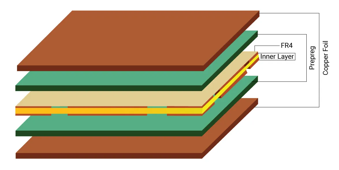
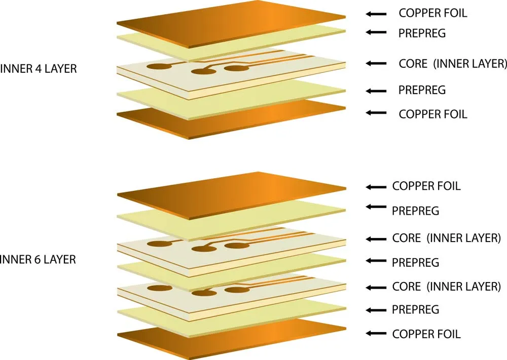
Copper foil thickness refers to the weight of copper per square foot on the PCB laminate, typically measured in ounces (oz/ft2), with common values ranging from 0.5 oz to 3 oz or more. Each increment roughly doubles the thickness: 1 oz is approximately 35 μm, while 2 oz reaches 70 μm before etching. In SMT assembly and PCB material selection, this parameter determines trace width requirements, current-carrying capacity, and heat dissipation properties. Thicker foils provide lower resistance paths for high-current signals, but they demand wider traces to maintain manufacturability, impacting overall board density. Engineers must balance these factors early in the design phase to avoid downstream assembly challenges.
The relevance to SMT stems from the assembly process's sensitivity to board flatness and thermal behavior. During solder paste printing and reflow, deviations in copper thickness across layers can induce warpage, misaligning fine-pitch components. Standard practices emphasize symmetric stackups where copper weights mirror between top and bottom layers to minimize these risks. For instance, unbalanced copper distribution exacerbates bow and twist, directly affecting pick-and-place accuracy and stencil registration.
Technical Principles: How Copper Thickness Affects SMT Assembly
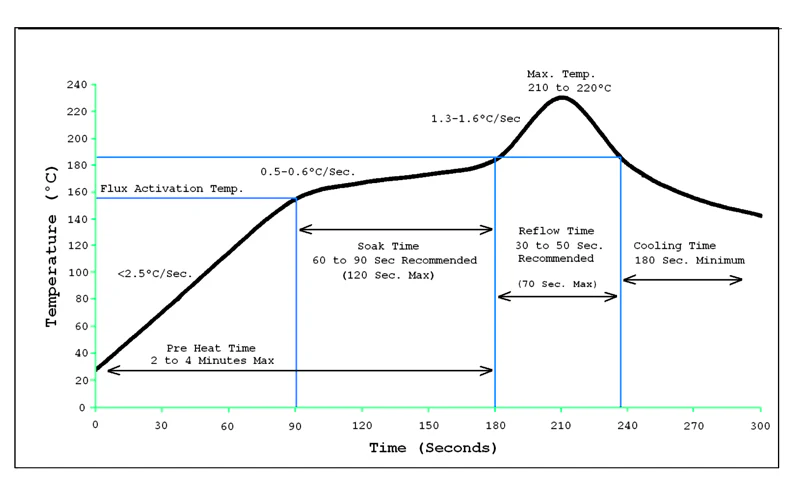
The primary Copper Foil Thickness effect SMT assembly appears in thermal management during reflow soldering. Thicker copper layers possess greater thermal mass and conductivity, causing traces to heat and cool at different rates compared to thinner dielectric regions. This leads to temperature non-uniformity across the board, potentially resulting in incomplete solder melting under components or excessive intermetallic growth. Engineers observe that SMT component assembly with thicker copper PCBs requires adjusted reflow profiles, often with longer preheat times to ensure uniform flux activation and solder flow.
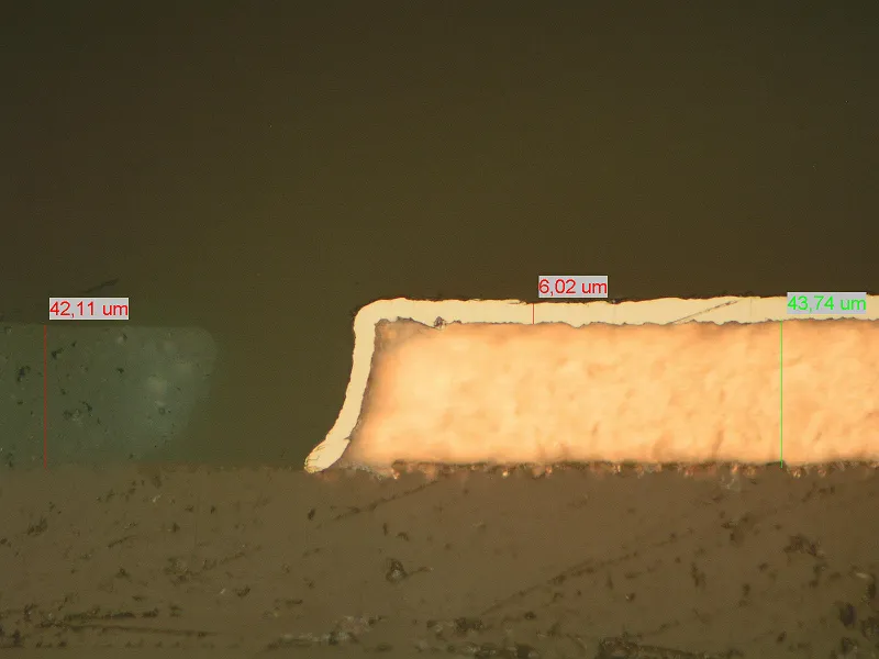
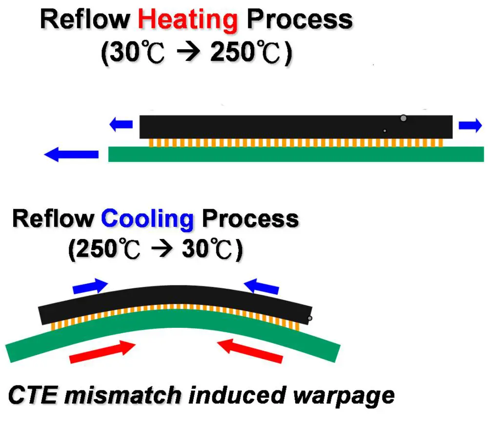
Warpage represents another key mechanism, driven by coefficient of thermal expansion (CTE) mismatch between copper and the substrate. Copper's CTE of about 17 ppm/°C contrasts with FR-4's 12-16 ppm/°C, and thicker foils amplify stress during temperature excursions from lamination to reflow peaks around 260°C. Asymmetric copper distribution, such as heavier weight on outer layers, induces convex or concave bowing, with measurements often exceeding allowable limits per industry test methods. This deformation shifts pad positions by microns, critical for 0.4 mm pitch BGAs, leading to open joints or bridges.
Electrically, thicker copper enhances current density tolerance, allowing narrower traces for space-constrained designs. However, etching thicker foils produces undercuts, reducing effective width and necessitating design rule adjustments like larger annular rings for vias. In high-layer-count boards, inner layer copper plating must meet minimum thicknesses post-etch to ensure via reliability under thermal cycling.
Per IPC-2221, current-carrying capacity scales with copper cross-section, justifying thicker foils for power rails exceeding 5 A, but this increases mechanical rigidity that can stress delicate SMT passives during board flexure.
Challenges with Thicker Copper in SMT Processes
SMT component assembly with thicker copper PCBs introduces specific hurdles in solder paste application and inspection. Wider traces from heavy copper demand stencils with adjusted aperture ratios to prevent paste starvation on fine features, while excess paste on broad pads risks bridging. Post-print, thicker copper's surface roughness, often higher in reverse-treated foils, can trap air pockets, compromising release and uniformity. Engineers troubleshoot by verifying stencil thickness, typically 0.1-0.15 mm, scales appropriately with pad sizes derived from copper weight.
Reflow soldering amplifies these issues through uneven heat transfer. Thick copper planes act as heat sinks, prolonging time-to-peak temperature under components and risking head-in-pillow defects where solder balls fail to coalesce fully. Conversely, isolated thin traces may overheat, promoting voiding. Profile optimization, including ramp-up rates of 1-3°C/s, mitigates this, but simulation tools help predict hotspots based on copper distribution.
Reliability post-assembly suffers if warpage persists. Cyclic thermal loads induce fatigue in solder joints, with thicker copper exacerbating CTE-driven shear stresses on low-profile components like 0201 resistors. Boards with heavy copper often require controlled impedance adjustments via dielectric thickness tweaks, complicating multilayer builds.
Best Practices for Copper Foil Selection in SMT PCB Design
Start with application requirements: default to 1 oz for signal integrity-focused boards under 3 A per trace, escalating to 2 oz for power distribution above 10 A. Use IPC-2221 charts to calculate trace widths, factoring 10-20°C allowable rise. For PCB design for SMT components, prioritize symmetric stackups, matching copper weights layer-pair wise to limit warpage below 0.75% per IPC test methods.
Incorporate copper balancing techniques like ground plane mirroring and fill patterns on inactive areas, ensuring no more than 20% asymmetry. Simulate warpage using finite element analysis early, inputting foil thicknesses and CTE values for reflow scenarios. Select electrodeposited (ED) foil for standard thicknesses and reverse-treated for high-frequency needs, though the latter suits lighter weights better.
For SMT assembly and PCB material selection, collaborate with fabricators on etch factor tolerances, as thicker foils (>2 oz) demand slower etchants to avoid trapezoidal profiles. Specify outer layers at least 1 oz heavier than inners if plated through-holes (PTH) dominate, compensating for plating buildup. Validate prototypes via shadow moiré at multiple temperatures to confirm flatness.
J-STD-001 guidelines underscore post-assembly inspection criteria, where copper thickness influences joint fillet formation and void limits.
Troubleshooting Common Issues in Thicker Copper SMT Assemblies
Engineers frequently encounter tombstoning in mixed copper weight boards, where small passives lift due to rapid copper cooling post-peak. Counter this by zoning heaters in reflow ovens or adding thermal vias under components. Bridging on power pads from thick copper traces responds to finer stencil apertures (80-90% of pad width) and low-residue pastes. Warpage-induced opens manifest as high-resistance joints on BGAs; measure bow/twist pre-assembly and route signals away from high-stress edges. If chronic, thin outer foils selectively or reinforce with frame carriers during reflow. Overheating in heavy copper power sections triggers delamination; distribute heat via buried planes and vias.
Conclusion
Selecting the right copper foil thickness optimizes Copper Foil Thickness effect SMT outcomes, balancing electrical robustness with assembly yield. Standard 1 oz suffices for most, but thicker options demand rigorous stackup symmetry, thermal profiling, and design rules. By adhering to principles like balanced distribution and standard-compliant calculations, engineers ensure reliable SMT component assembly with thicker copper PCBs. Proactive simulation and testing minimize risks, yielding durable boards ready for field deployment.
FAQs
Q1: What is the Copper Foil Thickness effect SMT reflow soldering?
A1: Thicker copper foils increase thermal mass, leading to slower heating and potential temperature gradients during reflow. This can cause incomplete wetting or defects like head-in-pillow in SMT joints. Adjust profiles with extended soaks and verify via thermocouples. Symmetric stackups reduce warpage contributions, ensuring uniform solder flow per assembly standards.
Q2: How does SMT component assembly with thicker copper PCBs impact yield?
A2: Thicker copper requires wider traces and pads, complicating stencil printing and risking bridges or starves. Warpage from asymmetry misaligns pick-and-place, dropping yields below 95%. Balance layers and simulate thermals to counteract. Post-reflow AOI catches issues early, maintaining high reliability.
Q3: What role does copper foil play in PCB design for SMT components?
A3: Copper thickness dictates current capacity and heat dissipation, influencing trace routing for dense SMT layouts. Thicker foils suit power but demand etch compensation to preserve tolerances. Symmetric designs per IPC guidelines prevent warpage, safeguarding fine-pitch assembly.
Q4: Why prioritize SMT assembly and PCB material selection with copper thickness?
A4: Material choices like low-CTE cores pair with copper weights to minimize reflow stresses. Thicker foils enhance dissipation but amplify warpage risks. Select based on current needs and validate flatness, optimizing overall assembly process control.
References
IPC-2221B — Generic Standard on Printed Board Design. IPC, 2003
IPC-6012E — Qualification and Performance Specification for Rigid Printed Boards. IPC, 2015
J-STD-001G — Requirements for Soldered Electrical and Electronic Assemblies. IPC, 2017