Introduction
In the compact world of mobile phone PCBs, component placement directly influences signal integrity, thermal performance, and power efficiency. Engineers face unique challenges due to limited board space, high-frequency signals, and dense populations of surface-mount devices. Effective strategies for SMT component placement ensure reliable operation under demanding conditions like multitasking processors and 5G connectivity. PCB routing guidelines become critical to minimize crosstalk and electromagnetic interference in these multilayer boards. By optimizing thermal component placement and power distribution, designers can prevent hotspots and voltage drops that degrade battery life. This article explores proven engineering approaches to achieve peak performance in mobile phone designs.
Why Component Placement Matters in Mobile Phone PCBs
Component placement in mobile phone PCBs determines the overall functionality and longevity of the device. Poor placement leads to excessive signal path lengths, increasing latency and noise in high-speed interfaces like USB and PCIe. Thermal mismanagement can cause components to throttle or fail prematurely, especially in processors and RF modules. Power distribution optimization prevents IR drops that affect analog circuits and memory stability. Adhering to PCB routing guidelines helps maintain impedance control across traces. Ultimately, strategic placement aligns with industry demands for smaller form factors without sacrificing reliability.
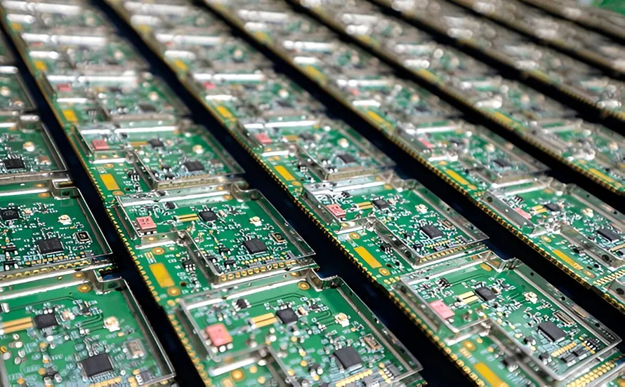
Mobile phones integrate diverse components, from tiny passives to large ICs, all vying for space on 4-10 layer boards. SMT component placement prioritizes grouping by function to streamline assembly and testing. Engineers must balance electrical, thermal, and mechanical constraints to meet performance specs. Neglecting these can result in yield losses during manufacturing or field failures. Standards like IPC-7351 provide land pattern guidelines that support precise placement for optimal solder joints.
Fundamental Technical Principles of Component Placement
Signal integrity relies on minimizing signal path lengths between high-speed components. Shorter paths reduce propagation delays and attenuation, crucial for data rates exceeding 10 Gbps in modern smartphones. Clock signals and differential pairs benefit most from proximity placement, as longer routes amplify skew and jitter. PCB routing guidelines recommend 45-degree bends over 90-degree to minimize reflections, with trace widths adjusted for controlled impedance. Vias introduce discontinuities, so limiting their use in critical nets preserves signal quality.
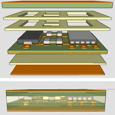
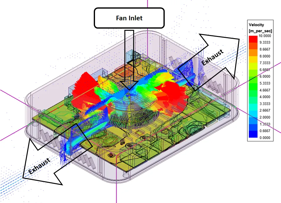
Thermal principles dictate placing heat-generating components away from sensitive analog areas. Processors and power amplifiers produce localized heat fluxes up to several watts per square centimeter. Convection and conduction paths must efficiently dissipate this to keep junction temperatures below 85°C in typical operation. Thermal component placement involves positioning vias under pads to transfer heat to inner planes or the opposite side. Material choices like copper thickness influence spreading resistance.
Power distribution optimization ensures uniform voltage delivery across the board. Decoupling capacitors placed within millimeters of IC power pins filter noise effectively. Wide power planes reduce resistance, but slots for shielding must not interrupt current flow. Engineers calculate plane resonance frequencies to avoid coupling with signal harmonics.
Best Practices for SMT Component Placement
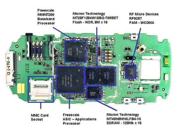
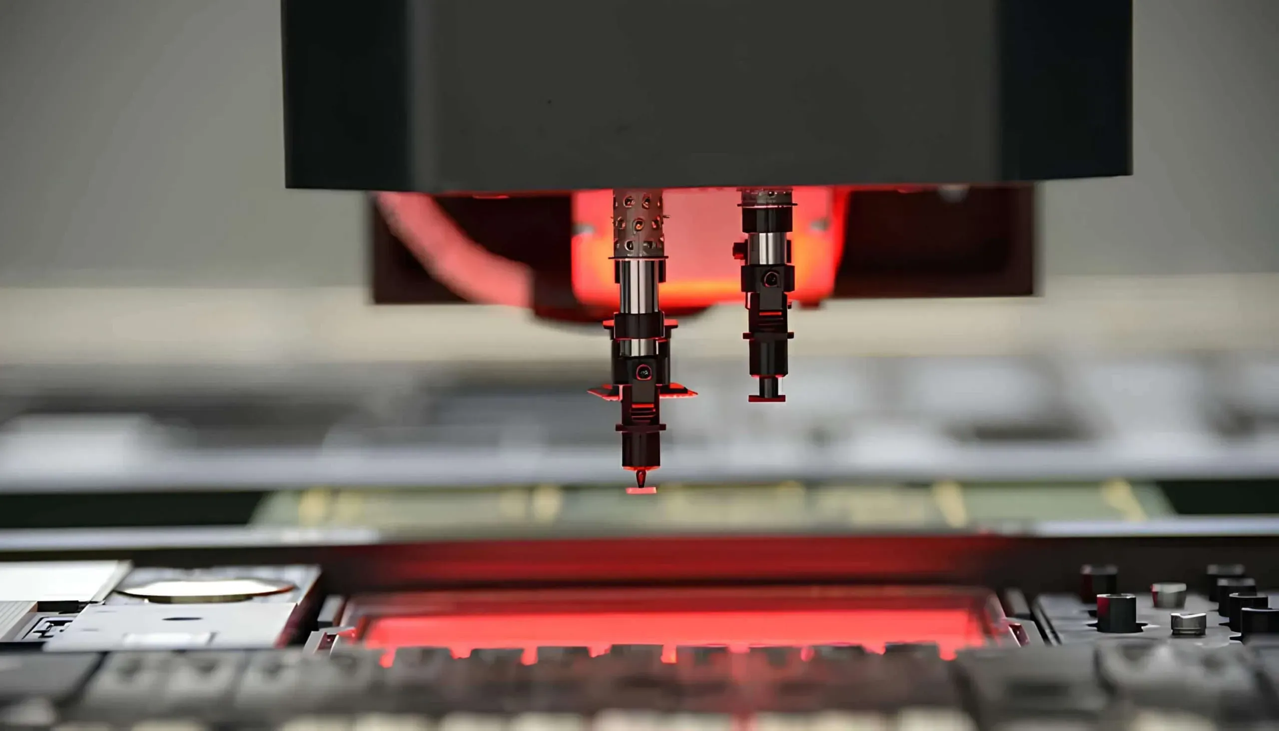
Start with functional grouping: place digital logic near processors, RF components near antennas, and passives adjacent to their loads. This SMT component placement strategy shortens interconnects and simplifies shielding. For BGA packages common in mobile SoCs, align balls under the die shadow to minimize stub lengths. Fiducials and panelization aids ensure alignment during pick-and-place, reducing defects per IPC-A-610 acceptability criteria.
Follow PCB routing guidelines by reserving outer layers for signals and inner for power/ground. High-current paths route first to secure wide traces, typically 0.5-1 mm for 1-2A loads. Minimize vias in power nets by using plane stitching. For minimizing signal path in DDR memory interfaces, position modules parallel to the controller with fly-by topology. Length matching within 5 mils prevents timing violations.
Thermal component placement prioritizes airflow paths aligned with device vents. Mount heat spreaders or embedded coins near hotspots, connected via thermal vias arrays. Space capacitors to avoid blocking convection currents. Simulate airflow to validate, ensuring deltas under 20°C between components.
Power distribution optimization employs multi-layer planes with interplane capacitance. Place bulk caps near voltage regulators and ceramics at loads. Segregate analog and digital supplies to curb noise. Decoupling schemes follow 1:10:100 nF ratios for frequencies up to GHz.
Implement design rules checks early, verifying clearances per J-STD-001 soldering requirements. Iterate layouts with electromagnetic field solvers to quantify crosstalk below -50 dB. Panel reviews catch mechanical issues like connector interference.
Advanced Strategies for High-Density Mobile PCBs
In 6G-era phones, minimizing signal path extends to waveguide transitions for mmWave. Place antennas and front-ends co-located, with shielding cans enclosing noisy sections. Hybrid integration of SiP modules reduces parasitics further.
For thermal management, leverage graphite sheets or TIMs under batteries, routing heat away from Li-ion cells. Dynamic placement adjusts for foldable designs, where flex-rigid transitions demand reinforced pads.
Power integrity analysis models PDN impedance below 10 mOhm up to 1 GHz. Via farms enhance return paths, optimizing distribution networks.
Troubleshooting Common Placement Issues
Excessive EMI often traces to unshielded clock lines near I/O. Reposition or add guards. Thermal runaway signals poor via thermal resistance; add more or enlarge. Voltage ripple indicates distant decoupling; relocate caps closer.
Yield drops from warpage call for symmetric placement balancing copper weight. Simulate reflow profiles per JEDEC J-STD-020 for moisture-sensitive devices.
Conclusion
Mastering component placement elevates mobile phone PCB performance across signal, thermal, and power domains. SMT component placement, adhered to PCB routing guidelines, minimizes signal path while enabling thermal component placement and power distribution optimization. Engineers applying these principles reduce risks and enhance reliability. Structured approaches grounded in standards deliver compact, efficient designs ready for production. Prioritize simulation and iteration for real-world success.
FAQs
Q1: What are the key PCB routing guidelines for minimizing signal path in mobile phones?
A1: PCB routing guidelines emphasize shortest paths for high-speed nets, using length-matched differential pairs and minimal vias. Prioritize outer layers for signals to ease manufacturing. Maintain 100-ohm impedance with appropriate widths and spacing. This approach reduces jitter in interfaces like MIPI, ensuring data integrity up to multi-Gbps rates. Follow symmetry to balance skew.
Q2: How does thermal component placement impact mobile phone PCB reliability?
A2: Thermal component placement directs heat away from sensitive areas via vias and planes, preventing derating. Position hotspots near edges for better dissipation. Arrays of 0.3 mm vias under BGAs improve conductance. This maintains Tj below thresholds, extending MTBF. Poor placement accelerates aging in polymers.
Q3: Why is power distribution optimization critical for SMT component placement?
A3: Power distribution optimization in SMT component placement ensures low-impedance paths, stabilizing supplies for mixed-signal ICs. Planes with stitching vias minimize drops under load transients. Close decoupling filters PDN noise effectively. This prevents resets in processors during peaks, vital for user experience.
Q4: What role do standards play in SMT component placement strategies?
A4: Standards like IPC-7351 guide land patterns for reliable SMT component placement, optimizing solder volume. They specify tolerances for high-density boards. Compliance boosts assembly yields and field performance.
References
IPC-7351 — Generic Requirements for Surface Mount Design and Land Pattern Standard. IPC, 2010
IPC-A-610 — Acceptability of Electronic Assemblies. IPC, 2017
J-STD-001 — Requirements for Soldered Electrical and Electronic Assemblies. IPC, 2020
J-STD-020 — Moisture/Reflow Sensitivity Classification for Nonhermetic Surface Mount Devices. JEDEC/IPC, 2014