Introduction
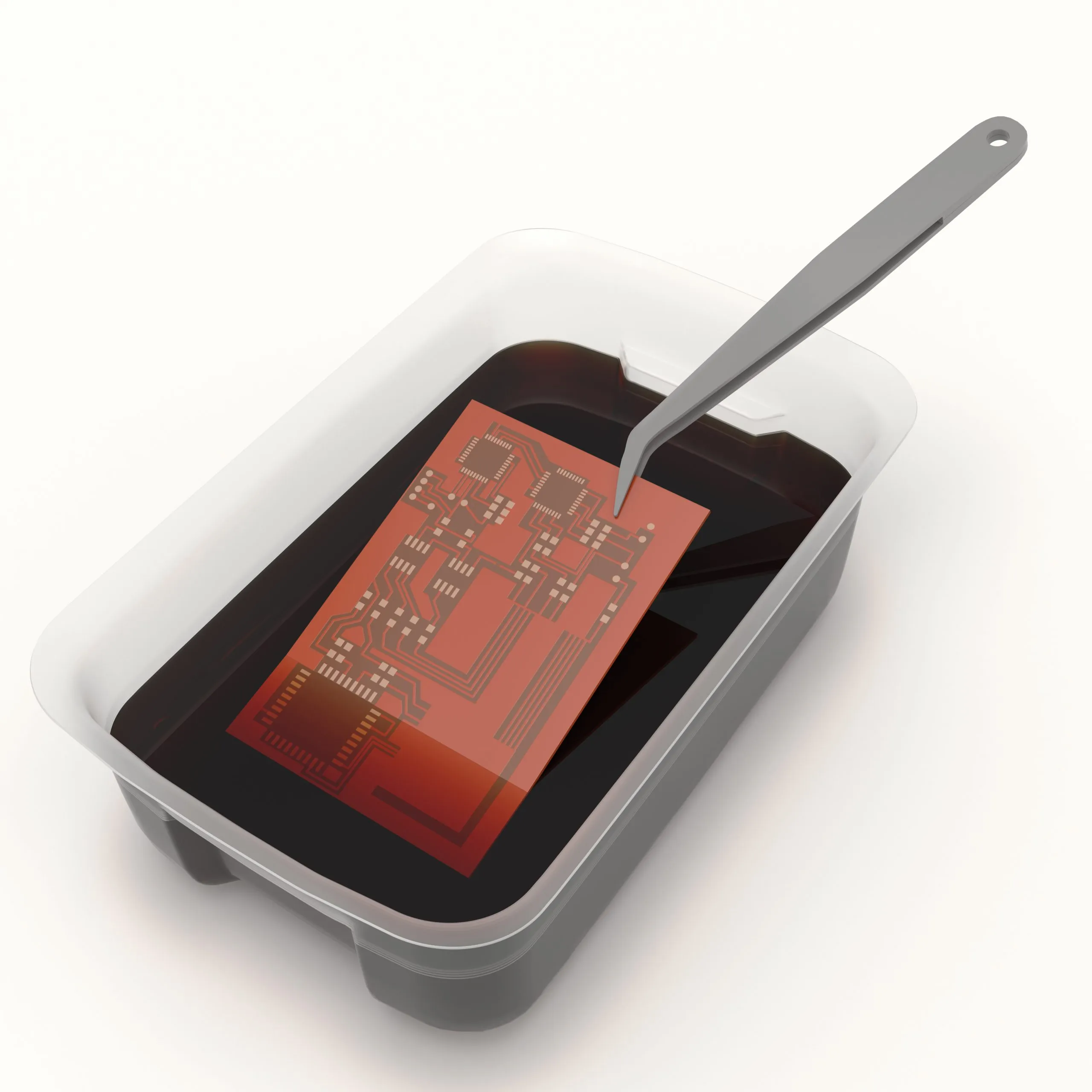
Electronic hobbyists often start their projects with simple copper clad boards, etching their own designs for custom circuits. Copper foil thickness plays a crucial role in these DIY efforts, influencing everything from etching success to circuit performance. Understanding copper clad board thickness helps hobbyists avoid common pitfalls like under-etched traces or overheated power lines. For projects like Arduino shields or sensor boards, selecting the right thickness ensures reliability without unnecessary complexity. This article explores the essentials of copper foil thickness, tailored for hands-on makers. Whether you are new to DIY PCB etching or refining your skills, grasping these concepts elevates your electronic hobby projects.
Many hobbyists grab the cheapest copper clad board without checking specs, leading to frustration during etching or testing. Thicker copper demands longer etch times and precise control, while thinner options allow finer traces ideal for dense Arduino projects. Industry standards guide professional designs, but hobbyists can apply similar principles for better results. This guide breaks down definitions, impacts, and practical tips. By the end, you will confidently choose copper thickness for your next build.
What Is Copper Foil Thickness and Why It Matters for Hobbyists
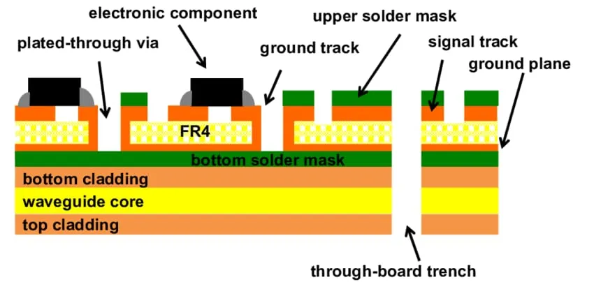
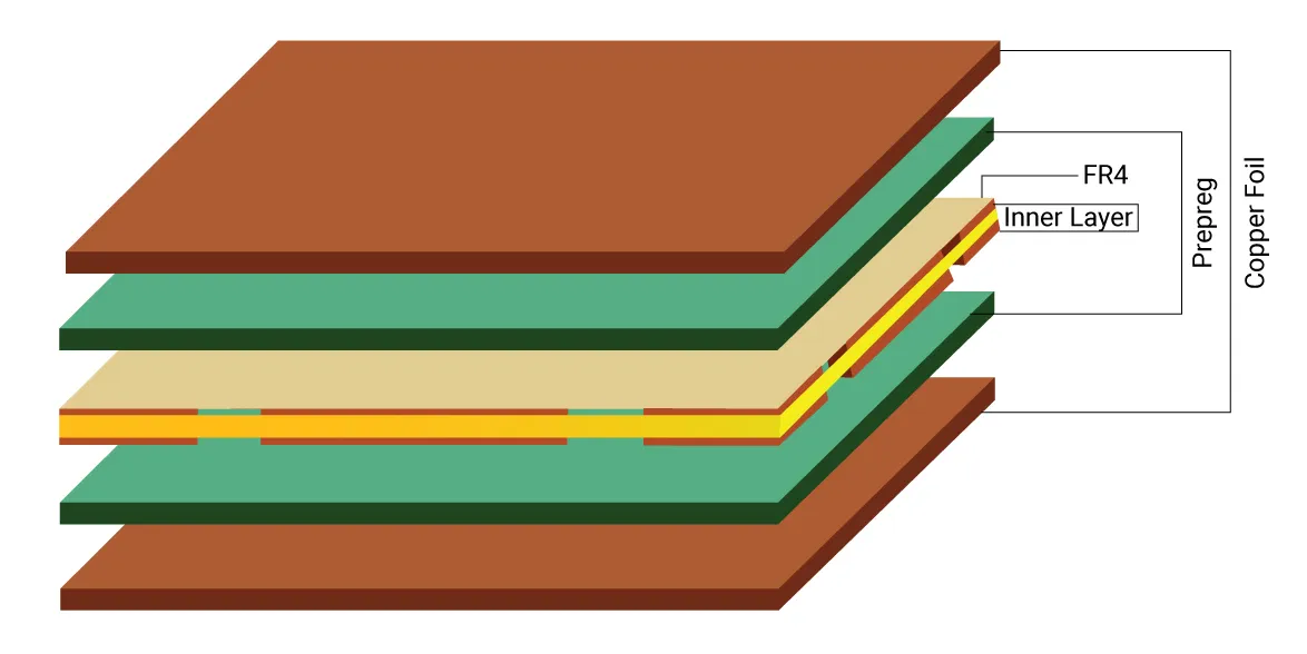
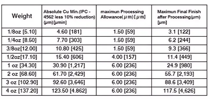
Copper foil thickness refers to the layer of copper laminated onto the substrate, typically FR4 glass epoxy in copper clad boards used by hobbyists. It is measured in ounces per square foot (oz/ft2), where 1 oz equals about 35 micrometers (μm) thick. Common options include 0.5 oz (17 μm), 1 oz (35 μm), and 2 oz (70 μm), with 1 oz being the standard for most DIY applications. This specification determines the board's ability to carry current, dissipate heat, and withstand etching processes.
For electronic hobbyists, copper clad board thickness directly affects project outcomes. In low-power Arduino projects, 1 oz suffices for signal traces, keeping resistance low without excess material. Thicker foils suit high-current paths, like motor drivers, preventing voltage drops. However, mismatched thickness leads to issues: thin copper overheats under load, while thick copper resists etchant penetration, causing uneven results in DIY PCB etching. Recognizing these trade-offs optimizes your designs.
Why does it matter beyond basics? Thicker foils increase mechanical strength but raise costs and etching difficulty. Hobbyists etching at home benefit from balancing thickness with project needs. For instance, prototype boards for sensors use standard 1 oz for versatility. Ignoring thickness risks failures in electronic hobby projects, from flickering LEDs to fried components.
Technical Principles of Copper Foil in PCBs
Copper foil in PCBs comes in two main types: electrodeposited (ED) and rolled annealed (RA). ED copper, prevalent in hobbyist copper clad boards, features a rougher surface for better adhesion during lamination. Its structure consists of pure copper grains formed electrochemically, providing uniform thickness across the sheet. RA copper offers smoother surfaces for high-frequency signals but is rarer in DIY stock. Understanding these helps predict etching behavior and performance.
Thickness impacts electrical properties fundamentally. Resistance per unit length decreases with thicker foil, following the formula R = ρL / (w t), where ρ is copper resistivity, L length, w width, and t thickness. For a given trace, doubling thickness halves resistance, vital for power distribution. Heat dissipation improves too, as thicker copper spreads thermal loads effectively. In multilayer boards, though hobbyists rarely build them, inner layers follow similar rules per IPC-6012 standards.
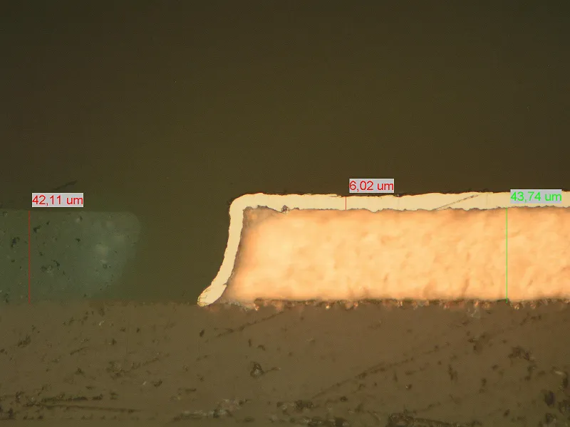
Etching dynamics hinge on thickness. Etchant attacks copper laterally and vertically, but thicker foils prolong the process, risking undercuts if not monitored. Hobbyists using ferric chloride note that 1 oz etches in 20-40 minutes, versus half for 0.5 oz. Uniformity suffers with variations, often 10-20% in budget boards. Precise temperature and agitation mitigate this.
Surface treatments like RTF (reverse treat foil) enhance peel strength, common in quality copper clad boards. Hobbyist boards may lack these, leading to delamination post-etching. Testing foil integrity before use prevents waste.
Choosing the Right Copper Thickness for Your Projects
Start with project requirements when selecting copper clad board thickness. For typical Arduino projects, like LED matrices or basic controllers, 1 oz provides ample capacity for currents under 1 A per trace. Calculate minimum widths using guidelines from IPC-2221, ensuring temperature rise stays below 20 °C. Wider traces compensate for thinner copper in low-power designs.
High-current electronic hobby projects demand thicker options. A motor shield might need 2 oz for power rails, reducing heat and voltage sag. Always prioritize external layers for heavy loads. Stock up on both 1 oz and 0.5 oz boards: thin for prototypes, standard for finals.
DIY PCB etching favors thinner copper for sharp traces. 0.5 oz cuts etching time, ideal for 0.2 mm lines in dense layouts. Use bubble etching or gentle agitation for best results. Post-etch inspection reveals issues early.
Best Practices and Experiments for Hobbyists
Follow these steps for reliable results. Verify copper thickness via supplier specs or simple tests before etching. Design traces with 0.5-1 mm width for 1 oz, scaling up for thickness changes. Simulate thermal performance mentally: thicker equals cooler.
Conduct a copper thickness experiment to build intuition. Etch identical trace patterns on 0.5 oz and 1 oz copper clad boards. Measure resistance across fixed lengths using a multimeter. Compare values; thicker shows lower ohms, confirming specs. Vary widths to see current limits by monitoring voltage drop under load. This hands-on approach refines your skills for future electronic hobby projects.
Adhere to IPC-2152 for current estimates in advanced designs. Maintain etch solutions fresh, agitating constantly. Solder masks are optional for prototypes but protect traces long-term. Store boards flat to avoid warpage.
For PCB for Arduino projects, integrate power planes if using thicker copper. Route signals away from high-current paths. Test iteratively: prototype on thin copper, scale to thicker for production runs.
Troubleshooting Common Issues
Overheating traces signal insufficient thickness or narrow widths. Widen paths or upgrade foil. Uneven etching points to thick copper or stale etchant; switch to thinner stock. Peeling foil indicates poor adhesion; clean substrates thoroughly pre-etch.
Warpage in finished boards arises from thermal mismatch, exacerbated by thick copper. Use symmetric layouts. Delamination post-soldering? Check foil quality.
Conclusion
Copper foil thickness fundamentally shapes successful electronic hobby projects. Standard 1 oz suits most DIY PCB etching and Arduino builds, balancing ease and performance. Thinner for precision, thicker for power: match to needs. Experiments and standards like IPC-2221 guide choices. Apply these insights for robust, frustration-free prototypes. Elevate your hobbyist game with informed selections.
FAQs
Q1: What is the standard copper clad board thickness for DIY projects?
A1: The standard copper clad board thickness is 1 oz per square foot, about 35 μm, ideal for most electronic hobby projects. It offers good current handling for Arduino prototypes while etching reliably at home. Thinner 0.5 oz works for fine traces, but verify with resistance tests post-etch. Always match to your power needs for best results.
Q2: How does copper thickness affect DIY PCB etching?
A2: Thicker copper, like 2 oz, extends etching time and risks undercuts in DIY PCB etching, demanding precise control. 1 oz balances speed and quality for hobbyists. Use fresh etchant and agitation; thinner foils yield sharper traces faster. Monitor progress to avoid over-etching.
Q3: What copper thickness is best for PCB for Arduino projects?
A3: For PCB for Arduino projects, 1 oz copper clad board thickness handles typical currents under 1 A effectively. Wider traces boost capacity if needed. It etches well at home and resists heat in sensor or display shields. Test loads to confirm.
Q4: Can I perform a copper thickness experiment at home?
A4: Yes, etch traces of known dimensions on different copper thicknesses, then measure resistance. Lower ohms indicate thicker foil in your copper thickness experiment. Apply small currents to check voltage drop. This verifies specs for reliable electronic hobby projects without special tools.
References
IPC-2221B — Generic Standard on Printed Board Design. IPC, 2003
IPC-6012E — Qualification and Performance Specification for Rigid Printed Boards. IPC, 2015
IPC-2152A — Standard for Determining Current Carrying Capacity in Printed Board Design. IPC, 2009