Introduction
Radio frequency printed circuit boards are essential in modern wireless communication systems, powering devices like smartphones, IoT modules, and radar systems. A critical factor in RF PCB design is core thickness, which directly impacts signal loss and overall performance. For electrical engineers, understanding how to optimize core thickness ensures better impedance control and minimizes signal degradation in high-frequency applications. This article explores the relationship between core thickness, signal loss, and wireless communication efficiency. It also covers key aspects of PCB material selection and RF circuit design to help engineers achieve reliable performance in antenna design and other RF applications. By following established industry standards, we aim to provide actionable insights for designing high-performance RF PCBs.
What Is Core Thickness in RF PCBs and Why It Matters
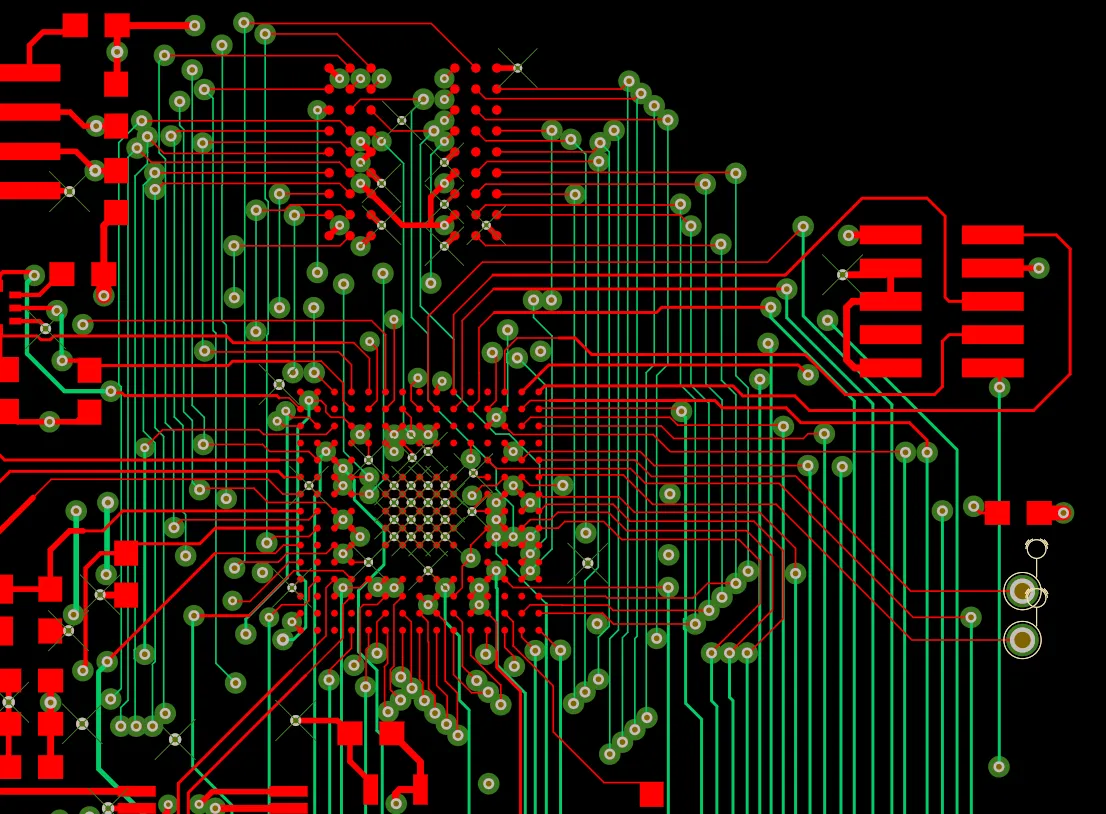
Core thickness in RF PCBs refers to the distance between conductive layers, typically the dielectric material separating copper traces in a multilayer board. This parameter is crucial because it influences the electromagnetic field distribution around traces, affecting signal integrity in wireless communication. In RF circuit design, even small variations in core thickness can alter impedance, leading to mismatches that cause signal loss. For applications operating at gigahertz frequencies, such as 5G networks or satellite systems, precise control of this thickness is vital. Incorrect thickness can result in increased dielectric losses and reduced efficiency in antenna design. Therefore, engineers must prioritize core thickness as a fundamental element of RF PCB design to ensure optimal performance and minimal signal degradation in high-frequency environments.
Technical Principles of Core Thickness and Signal Loss
In RF PCB design, core thickness affects signal loss through several mechanisms. The dielectric material between conductive layers interacts with high-frequency signals, and its thickness determines the capacitance and inductance of transmission lines. Thicker cores can increase signal loss due to longer signal paths through the dielectric, which often has inherent loss properties defined by its dissipation factor. Conversely, thinner cores may reduce dielectric losses but can complicate impedance control, as small manufacturing variations have a larger relative impact.
Signal loss in wireless communication systems primarily occurs due to dielectric loss and conductor loss. Dielectric loss depends on the material's properties and frequency, while conductor loss relates to skin effect, where high-frequency signals travel near the surface of conductors, increasing resistance. Core thickness influences the field distribution, impacting how much signal energy is lost to the dielectric. For instance, a thicker core may spread the electric field, potentially increasing losses if the material has a high dissipation factor.
Impedance control is another critical aspect tied to core thickness. In RF applications, maintaining a specific characteristic impedance, often 50 ohms, is necessary for efficient power transfer. The thickness of the dielectric directly affects this impedance, as it alters the capacitance between the trace and ground plane. Industry standards like IPC-2141A provide guidelines for calculating controlled impedance based on dielectric thickness and material properties, ensuring engineers can predict and mitigate signal loss effectively.
Related Reading: Choosing PCB Copper Weight: 1oz vs. 2oz for Optimal Performance
Impact of Core Thickness on Antenna Design and Wireless Communication
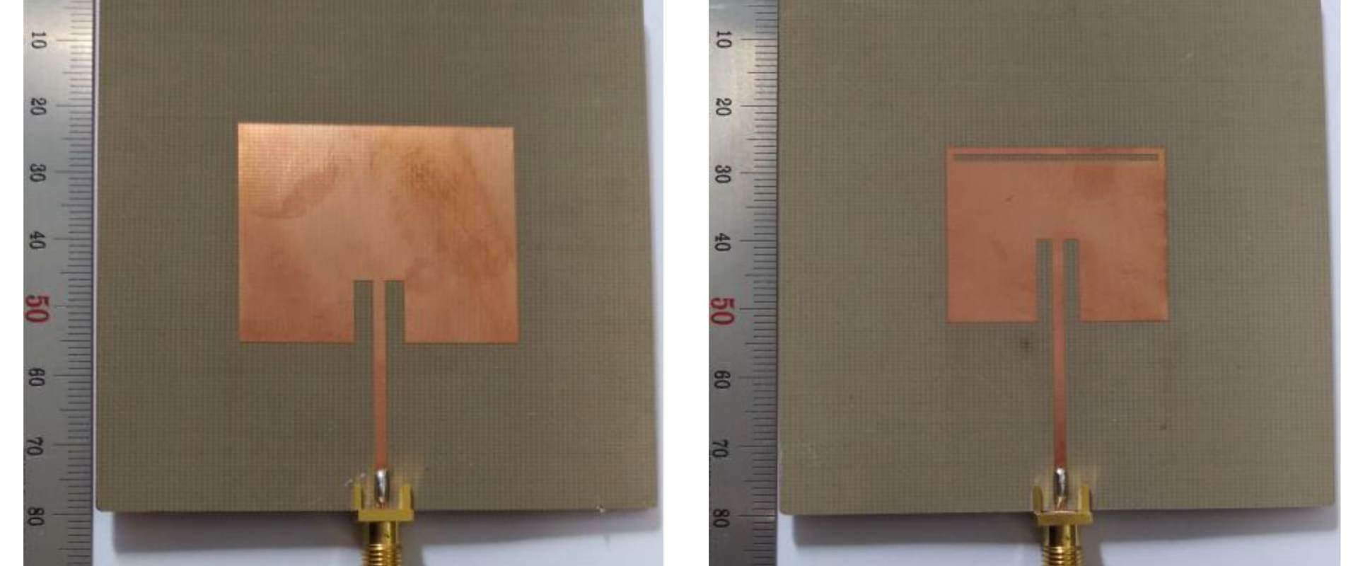
Antenna design for wireless communication heavily relies on precise RF PCB design. Core thickness influences the performance of embedded or PCB-integrated antennas by affecting the radiation pattern and efficiency. A mismatched core thickness can detune the antenna, leading to poor signal transmission and reception. For instance, in patch antennas commonly used in wireless systems, the dielectric thickness determines the resonant frequency and bandwidth. Engineers must carefully select a core thickness that aligns with the desired operating frequency to minimize signal loss.
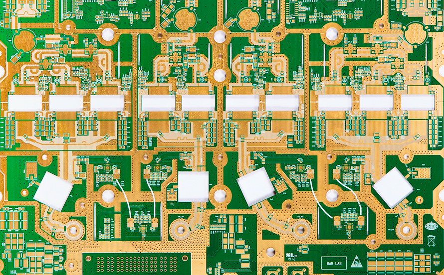
In multilayer RF PCBs, core thickness also impacts the coupling between layers, which can introduce unwanted noise or crosstalk in wireless communication circuits. A balanced approach is necessary to avoid overly thick cores that increase losses or overly thin cores that risk manufacturing inconsistencies. Adhering to standards such as IPC-6012E ensures that the specified core thickness meets performance and reliability requirements for high-frequency applications.
Practical Solutions for Optimizing Core Thickness in RF PCB Design
Selecting the appropriate core thickness for RF PCBs requires a systematic approach. Below are key strategies to minimize signal loss and ensure effective wireless communication performance.
- Understand Frequency Requirements: Higher frequencies in RF circuit design demand thinner dielectric layers to reduce signal loss. Consult design guidelines from standards like IPC-2141A to match core thickness with the operating frequency.
- Choose Suitable Materials: PCB material selection plays a vital role in managing signal loss. Materials with low dielectric constants and low dissipation factors are preferred for RF applications. Ensure the chosen material supports the required core thickness for impedance control.
- Simulate Impedance Early: Use simulation tools compliant with industry standards to predict how core thickness affects characteristic impedance. Adjust the thickness to achieve the target impedance, often 50 ohms, for optimal power transfer.
- Consider Manufacturing Tolerances: Thinner cores are more susceptible to variations during fabrication. Refer to IPC-6012E for acceptable tolerances to ensure consistent performance across production batches.
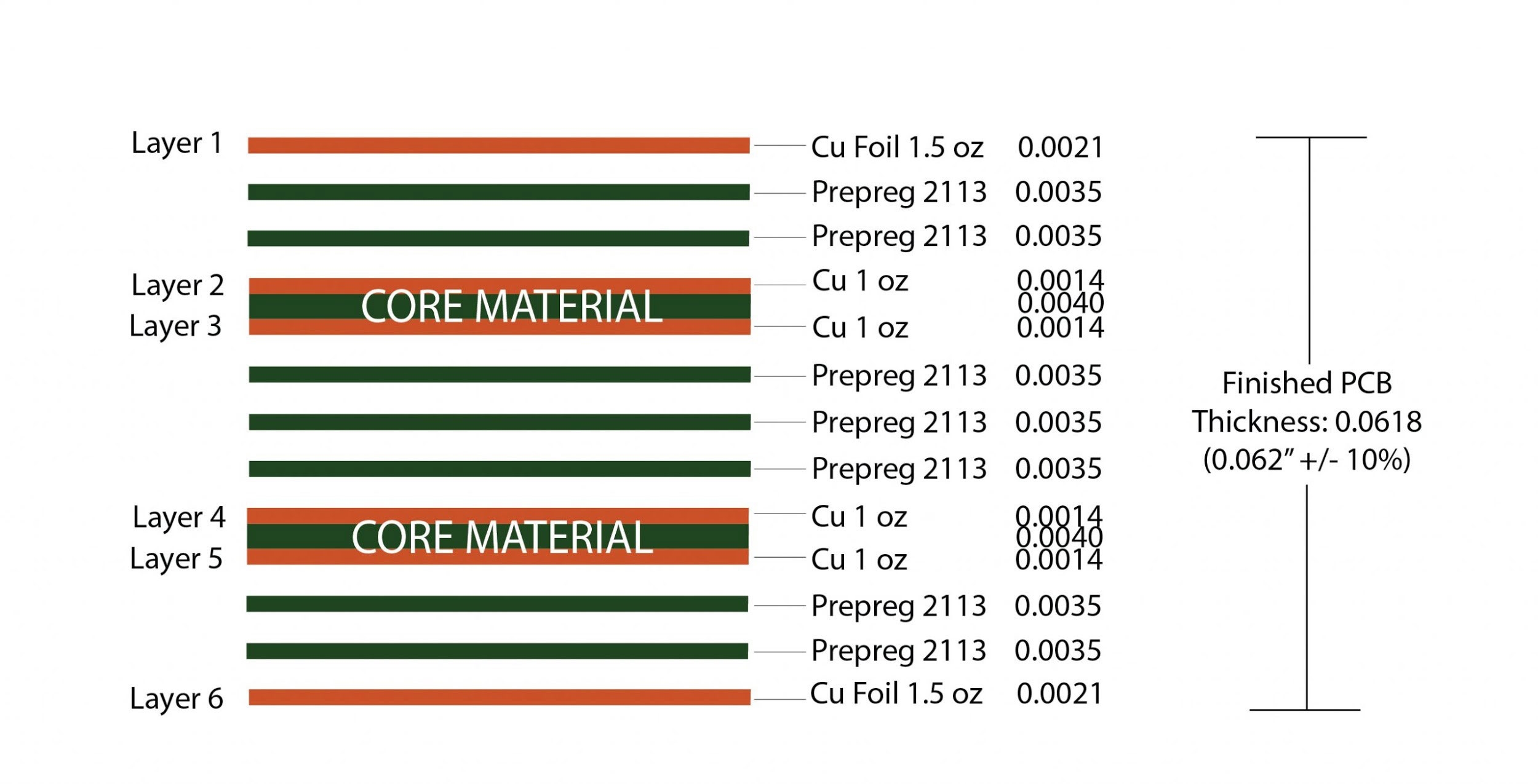
- Balance Stackup Design: In multilayer RF PCBs, distribute core thicknesses to minimize crosstalk while maintaining signal integrity. A well-planned stackup prevents excessive dielectric losses in critical signal layers.
By integrating these practices, engineers can optimize core thickness to enhance performance in wireless communication and antenna design projects. Collaboration with fabrication teams is also essential to confirm that the selected thickness aligns with manufacturing capabilities and standards.
Related Reading: RF PCB Design for Beginners: A Complete Introductory Guide
Best Practices for PCB Material Selection in RF Applications
PCB material selection is closely tied to core thickness and signal loss in RF PCB design. The dielectric material's properties, such as dielectric constant and dissipation factor, directly influence how core thickness impacts performance. Materials with lower dielectric constants allow for wider traces at a given impedance, which can reduce conductor losses. Similarly, a low dissipation factor minimizes dielectric losses, especially at higher frequencies.
Common material categories for RF applications include high-frequency laminates that offer stable performance across a range of core thicknesses. When selecting a material, engineers should evaluate its compatibility with the desired thickness and frequency range. Standards like IPC-4101E provide specifications for laminate materials, ensuring they meet the thermal and electrical requirements of RF circuit design. Additionally, thermal expansion properties must be considered to prevent delamination or warpage under operating conditions, as outlined in IPC-A-600K.
Troubleshooting Signal Loss Issues Related to Core Thickness
Signal loss in RF PCBs can often be traced back to improper core thickness or material choices. If an RF circuit exhibits higher-than-expected loss, engineers should first verify the actual core thickness against the design specification using measurement techniques outlined in IPC-A-600K. Deviations may indicate manufacturing errors that affect impedance control.
Another common issue is impedance mismatch caused by incorrect assumptions about dielectric properties at specific thicknesses. Reassessing the stackup design and simulating the impedance can help identify discrepancies. If losses persist, consider testing alternative core thicknesses or materials with lower dissipation factors to improve performance. Documenting these adjustments ensures compliance with quality management systems like ISO 9001:2015, providing a traceable record of design iterations.
In antenna design, signal loss may manifest as reduced range or efficiency. Adjusting the core thickness to retune the antenna to the target frequency often resolves such issues. Engineers should also inspect for crosstalk or interference in multilayer boards, as improper core thickness between layers can exacerbate these problems.
Conclusion
Core thickness is a pivotal factor in RF PCB design, directly influencing signal loss and performance in wireless communication systems. By understanding the technical principles behind dielectric interactions and impedance control, engineers can make informed decisions to optimize core thickness. Practical strategies, such as aligning thickness with frequency requirements and selecting appropriate materials, ensure minimal signal degradation. Adherence to industry standards like IPC-6012E and IPC-2141A guarantees reliability and consistency in high-frequency applications. Whether designing antennas or complex RF circuits, prioritizing core thickness and material properties is essential for achieving efficient and robust wireless solutions.
FAQs
Q1: How does core thickness affect signal loss in RF PCB design?
A1: Core thickness impacts signal loss by influencing dielectric and conductor losses in RF PCB design. Thicker cores can increase dielectric losses due to extended signal paths, while thinner cores may complicate impedance control. Selecting an optimal thickness based on frequency and material properties minimizes loss, ensuring efficient performance in high-frequency applications.
Q2: What role does PCB material selection play in managing core thickness for wireless communication?
A2: PCB material selection is critical for managing core thickness in wireless communication. Materials with low dielectric constants and dissipation factors reduce signal loss at specific thicknesses. Choosing the right material ensures stable impedance and minimizes losses, supporting reliable performance in RF applications as per industry standards.
Q3: Why is impedance control important in RF circuit design with varying core thicknesses?
A3: Impedance control is vital in RF circuit design to ensure efficient power transfer and minimal signal reflection. Core thickness directly affects characteristic impedance, and mismatches can lead to significant losses. Precise control, guided by standards, maintains signal integrity across varying thicknesses in high-frequency circuits.
Q4: How can antenna design benefit from optimized core thickness in RF PCBs?
A4: Optimized core thickness in RF PCBs enhances antenna design by ensuring proper resonance and efficiency. Correct thickness aligns the antenna with the target frequency, reducing signal loss and improving radiation patterns. This results in better range and performance for wireless communication systems.
References
IPC-6012E — Qualification and Performance Specification for Rigid Printed Boards. IPC, 2020.
IPC-2141A — Design Guide for High-Speed Controlled Impedance Circuit Boards. IPC, 2004.
IPC-4101E — Specification for Base Materials for Rigid and Multilayer Printed Boards. IPC, 2017.
IPC-A-600K — Acceptability of Printed Boards. IPC, 2020.
ISO 9001:2015 — Quality Management Systems. ISO, 2015.