Introduction
In modern electronics, printed circuit boards face increasing thermal challenges from high-power components like power converters and LEDs. Effective thermal management ensures reliability while keeping costs low, a critical balance for electric engineers designing budget-conscious products. Cost effective PCB thermal management involves strategic stackup decisions that enhance heat dissipation without excessive material or manufacturing expenses. This article explores affordable PCB materials for heat dissipation, optimizing thermal vias for cost, and other tactics like reducing copper weight for cost savings. Engineers can achieve budget friendly PCB stackup configurations that meet performance needs through informed design choices rooted in manufacturing realities.
Understanding PCB Stackup and Its Role in Thermal Management
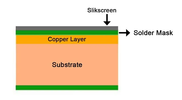
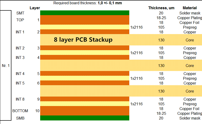
PCB stackup refers to the layered arrangement of copper foils, dielectrics, and cores that form the board's structure. Each layer influences heat flow, with copper planes acting as primary heat spreaders and dielectrics determining insulation and thermal conductivity. Poor stackup design leads to hotspots, delamination, or reduced lifespan, especially under IPC-6012E qualification standards for rigid boards. Thermal vias connect layers to transfer heat vertically, while material selection impacts overall dissipation efficiency.
For electric engineers, stackup optimization starts with analyzing power density and operating temperatures. Standard FR-4 materials offer a baseline for affordable PCB materials for heat dissipation, providing sufficient performance for many applications at lower costs than high-end laminates. Balancing layer count and thickness prevents warpage, ensuring the board maintains flatness during assembly and operation.
Related Reading: Mastering 12-Layer PCB Stackups for High-Performance High-Speed Designs
Key Principles of Heat Dissipation in PCB Stackups
Heat in PCBs generates primarily from conductors carrying current, with dissipation occurring via conduction, convection, and radiation. Copper's high thermal conductivity, around 400 W/mK, makes it ideal for spreading heat laterally across planes. Dielectric materials like FR-4 have lower conductivity, typically 0.3 W/mK, so stackups must maximize copper exposure to surfaces or heatsinks.
Thermal resistance in stackups depends on layer sequencing; placing power planes adjacent to components reduces path lengths for heat escape. Engineers must consider via thermal resistance, where barrel diameter and plating thickness play roles in conductance. Optimizing these elements aligns with J-STD-020E guidelines for moisture sensitivity, indirectly supporting thermal stability by preventing reflow-induced defects.
Budget constraints often limit exotic fillers in dielectrics, pushing reliance on geometry over materials. Symmetric stackups, with balanced copper on top and bottom, minimize CTE mismatch stresses that exacerbate thermal issues.
Affordable Materials for Heat Dissipation in Stackups
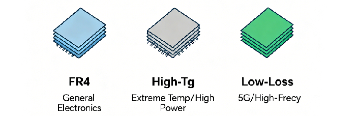
Selecting affordable PCB materials for heat dissipation begins with standard epoxy-based laminates like FR-4, which balance cost and performance for most mid-power designs. These materials exhibit Tg values suitable for lead-free soldering, avoiding the premium of high-Tg alternatives unless extreme temperatures demand them. Thinner cores reduce material volume, lowering costs while maintaining adequate insulation between planes.
Hybrid stackups incorporate cost-effective high-copper layers only where needed, such as inner planes for heat spreading. Engineers evaluate glass transition temperature and Z-axis expansion to ensure compatibility under thermal cycling. Factory processes favor these materials for their predictability in lamination and drilling, streamlining production.
Reducing overall board thickness via controlled impedance dielectrics cuts resin usage without sacrificing dissipation paths. This approach supports budget friendly PCB stackup by prioritizing volume manufacturing efficiencies.
Related Reading: Solving Thermal Challenges in PCB Prototyping: Techniques for Heat Dissipation
Optimizing Thermal Vias for Cost Savings
Thermal vias serve as vertical conduits, transferring heat from surface components to inner planes or the opposite side. Optimizing thermal vias for cost involves using arrays of smaller vias rather than large singles, as smaller drills reduce fabrication time and tool wear. Staggered patterns improve density without increasing annular ring sizes, enhancing conductance per unit area.
Unfilled vias suffice for many applications, avoiding the added expense of conductive or epoxy fills reserved for high-reliability boards. Plating thickness per IPC-6012E ensures void-free barrels, maintaining low thermal resistance at minimal copper use. Engineers calculate via pitch based on component footprint, aiming for 10-20% surface coverage to balance airflow and cost.
Post-drill cleaning prevents resin smear, preserving via performance during plating. This method yields cost effective PCB thermal management by leveraging standard via processes over specialized techniques.
Reducing Copper Weight for Cost Savings in Stackups
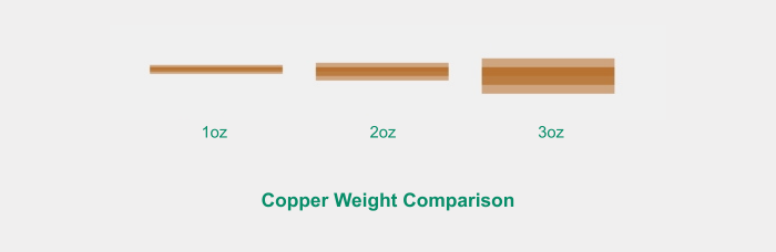
Reducing copper weight for cost savings targets non-critical traces, using 1 oz/ft2 instead of 2 oz where current demands allow. Thinner copper lowers material costs and etching expenses, as heavier foils require longer exposure times and more aggressive chemistries. Inner layers benefit most, retaining full weight for heat spreading while outer layers slim down for signal integrity.
Panel utilization improves with lighter weights, reducing waste in high-volume runs. Engineers verify ampacity using design guidelines, ensuring no hotspots from undersized conductors. This tactic integrates seamlessly into budget friendly PCB stackup, freeing budget for via enhancements or additional planes.
Differential etching controls prevent over-etching in reduced-weight foils, maintaining trace integrity. Manufacturing yields rise as thinner foils handle better in handling and lamination.
Best Practices for Budget-Friendly Stackup Design
Start with a 4-6 layer stackup for most thermal needs, dedicating one full plane to ground for return paths and heat sinking. Position power and ground planes adjacently to form a thermal capacitor, minimizing impedance and resistance. Simulate stackup symmetry to comply with warpage limits in IPC-A-600K acceptability criteria.
Incorporate microvias selectively for high-density areas, reserving through-vias for thermal roles to cut blind/buried costs. Factory-driven insights emphasize prepreg selection for uniform flow, ensuring void-free lamination that aids heat paths. Test prototypes with infrared imaging to validate dissipation before full production.
Via tents or plugs protect against solder wicking, a low-cost step enhancing reliability. Collaborate early with fabricators on DFM rules to refine stackup for manufacturability.
Common Challenges and Troubleshooting in Thermal Stackups
Engineers often encounter hotspots from asymmetric stackups, leading to CTE-induced failures. Symmetric configurations distribute stresses evenly, preventing barrel cracks in vias. Delamination risks rise with mismatched materials; sticking to compatible FR-4 grades mitigates this.
Over-reliance on heavy copper inflates costs without proportional gains; hybrid approaches yield better ROI. Air voids from poor lamination trap heat, detectable via cross-section analysis per IPC-TM-650 methods. Iterative design refines these issues cost-effectively.
Conclusion
Cost effective PCB thermal management hinges on smart stackup choices like affordable materials, optimized vias, and judicious copper reduction. These strategies deliver budget friendly PCB stackup that upholds performance under real-world loads. Electric engineers benefit from standard-aligned practices that enhance reliability without premium pricing. Implementing these principles streamlines design-to-production, ensuring thermal success on a budget.
FAQs
Q1: What are the main affordable PCB materials for heat dissipation in stackups?
A1: Standard FR-4 laminates provide cost effective PCB thermal management with adequate thermal conductivity for most applications. They offer reliable performance at lower costs than ceramic-filled alternatives, supporting symmetric stackups that minimize warpage. Factory processes favor FR-4 for its compatibility with standard drilling and plating, ensuring high yields in budget friendly PCB stackup designs.
Q2: How can optimizing thermal vias reduce costs without compromising performance?
A2: Optimizing thermal vias for cost uses arrays of small, staggered vias instead of large singles, cutting drill time and material use. This maintains low thermal resistance while adhering to plating standards like IPC-6012E. Unfilled vias suffice for many boards, enhancing heat transfer to planes in a budget friendly PCB stackup.
Q3: Is reducing copper weight viable for cost savings in thermal management?
A3: Reducing copper weight for cost savings applies to outer layers, using 1 oz where possible while keeping inner planes heavier for dissipation. This lowers etching and material expenses without hotspots, per design guidelines. It integrates well into cost effective PCB thermal management for mid-power electronics.
Q4: What makes a stackup budget friendly yet thermally efficient?
A4: A budget friendly PCB stackup features 4-6 layers with dedicated heat-spreading planes, symmetric construction, and optimized vias. Affordable FR-4 materials and selective copper weights balance costs and performance. Manufacturing insights ensure DFM compliance for reliable thermal paths.
References
IPC-6012E — Qualification and Performance Specification for Rigid Printed Boards. IPC, 2017
J-STD-020E — Moisture/Reflow Sensitivity Classification. JEDEC, 2014
IPC-A-600K — Acceptability of Printed Boards. IPC, 2020