Introduction
Through-hole vias remain a cornerstone in PCB design for applications requiring robust mechanical and electrical connections across multiple layers. These vias, which extend fully from one board surface to the other, offer reliable performance in power distribution and high-current paths but often contribute significantly to PCB manufacturing cost due to the intensive drilling and plating processes involved. Engineers face the challenge of optimizing through-hole via cost without compromising signal integrity or thermal management. Via design optimization plays a critical role in minimizing PCB cost, especially in mid-volume production runs where fabrication expenses dominate the budget. This article explores practical strategies to balance these demands, drawing on established engineering principles to help electric engineers achieve efficient designs.
Understanding Through-Hole Vias and Their Cost Implications
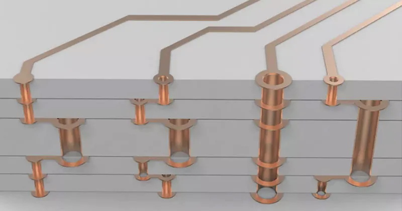
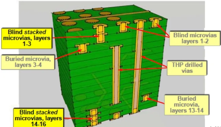
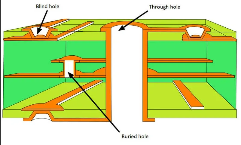
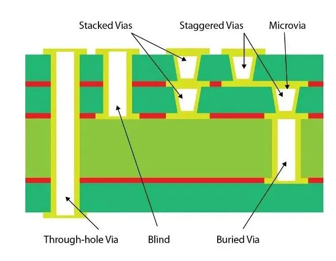
Through-hole vias consist of a drilled hole plated with copper to form an interconnect that spans the entire board thickness, enabling interlayer connections in multilayer PCBs. Unlike blind or buried vias, they require processing through all layers, which increases fabrication time and material usage. The primary cost drivers stem from mechanical drilling, electroless and electrolytic plating, and subsequent inspection steps to ensure barrel quality. In high-density designs, excessive through-hole vias can elevate PCB manufacturing cost by prolonging drill cycles and risking defects like dog-boning or plating voids. Engineers must weigh these factors against performance needs, such as low resistance for power planes or mechanical strength for component leads. Understanding these basics allows for targeted via design optimization from the outset.
The relevance of through-hole vias persists in cost-sensitive applications like industrial controls and automotive electronics, where HDI alternatives may exceed budgets. Standard board thicknesses, typically 1.6 mm, combined with via diameters around 0.3 mm, set baseline costs, but deviations amplify expenses. Factory processes prioritize standardization to control variability, making non-standard via sizes a hidden cost multiplier. By aligning designs with common fabrication capabilities, teams can reduce through-hole via cost while maintaining compliance with quality benchmarks.
Key Factors Influencing Through-Hole Via Cost
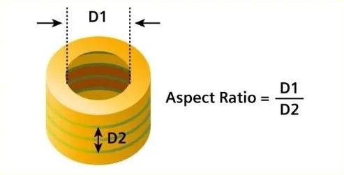
Several interrelated factors dictate through-hole via cost during PCB manufacturing. Drill diameter is paramount; smaller holes demand precision tooling and slower feed rates to avoid breakage or misalignment, directly inflating cycle times. Aspect ratios, defined as board thickness divided by via diameter, should stay below recommended limits to ensure uniform plating, as higher ratios lead to incomplete copper deposition and yield losses. Material choices, such as FR-4 laminates, interact with via design by influencing drill wander and heat dissipation during fabrication. Density of vias also matters, as clustered placements complicate panel utilization and increase handling risks.
Plating processes add another layer of expense, with through-hole vias requiring more copper deposition than surface-level interconnects. Electrolytic plating baths must maintain consistent current density across all holes, a challenge in boards with varying via populations. Post-plating steps like solder mask application and tenting further impact costs if vias are oversized or poorly spaced. Electrical testing verifies continuity and shorts, consuming time proportional to via count. Engineers optimizing for minimal PCB cost focus on these variables to streamline production without sacrificing reliability.
IPC-6012 provides qualification criteria for rigid printed boards, emphasizing via geometry tolerances that influence manufacturing efficiency. Adhering to such guidelines prevents costly rework while enabling economical designs.
Strategies for Via Design Optimization
Effective via design optimization begins with minimizing the number of through-hole vias through intelligent routing. Consolidate connections by using larger power and ground planes, reserving through-holes for essential high-current or mechanical anchors. Select standard drill sizes, such as 0.4 mm or 0.6 mm, which align with factory tooling and reduce setup costs compared to custom dimensions. Increase via diameter where signal integrity permits to lower aspect ratios and plating demands, thereby cutting through-hole via cost. Spacing vias adequately prevents drill bit deflection and supports efficient panelization for batch processing.
Tenting solder mask over non-plated vias saves on resist material and improves cleanliness during assembly. Filled vias, using conductive or non-conductive epoxy, enhance thermal performance in dense areas but require evaluation against budget constraints due to added material steps. Simulate via stub effects in high-speed designs to justify their use over shorter alternatives, ensuring performance matches cost savings. Iterative design reviews with fabrication feedback loops refine these choices.
Panel-level considerations amplify savings; designing for standard panel sizes with optimal via distribution maximizes yield per panel. Factory-driven insights highlight that symmetric via placement aids warpage control during lamination, indirectly lowering scrap rates.
Exploring Via Alternatives for Cost Reduction
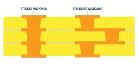
While through-hole vias excel in simplicity, via alternatives offer pathways for minimizing PCB cost in specific scenarios. Blind vias, connecting only outer to inner layers, eliminate stubs for better signal integrity but demand sequential lamination, potentially raising expenses for complex stacks. Buried vias, fully internal, further reduce surface clutter yet require advanced buildup processes unsuitable for budget boards. Microvias, laser-drilled for HDI, provide high density at premium costs due to specialized equipment.
Pressed or molded vias present niche options for high-volume runs, bypassing electroplating via mechanical forming, though tooling investments limit their use. Surface-mount technologies like embedded components can obviate some vias entirely, redirecting budget to assembly efficiencies. Engineers evaluate these via alternatives based on layer count, speed requirements, and production volume. For many mid-range designs, hybrid approaches blending through-holes with blinds yield the best cost-performance ratio.
J-STD-001 outlines soldering requirements that influence via land designs, ensuring alternatives maintain assembly reliability without excess cost.
Best Practices for Implementation in Electric Engineering Projects
Implement via design optimization through a structured workflow starting with stackup planning. Define via requirements early via electrical modeling to predict inductance and capacitance, avoiding over-provisioning. Collaborate with fabricators on design for manufacturability (DFM) rules, targeting drill-to-copper clearances per industry norms. Use via-in-pad techniques judiciously for BGA footprints to conserve space without proliferating holes.
Monitor thermal aspects, as through-hole vias aid heat dissipation but cluster poorly if unchecked. Prototype testing validates cost reductions, focusing on metrics like fabrication yield and assembly defects. Document rationale for via choices in design files to facilitate procurement and revisions.
Conclusion
Balancing through-hole via cost with performance demands a holistic approach encompassing geometry, density, and alternatives. Engineers achieve minimizing PCB cost by leveraging standard sizes, reducing counts, and aligning with fabrication realities. These strategies uphold reliability across applications while curbing expenses. Prioritizing via design optimization ensures competitive designs without undue trade-offs. Future trends may shift toward advanced alternatives, but through-hole vias will endure for their proven value.
FAQs
Q1: How can engineers reduce through-hole via cost in high-density PCBs?
A1: Focus on via design optimization by selecting larger standard diameters to ease drilling and plating, while minimizing total count through plane usage. Group vias for efficient panelization and adhere to aspect ratio limits for uniform copper deposition. Factory feedback on DFM rules prevents costly iterations, achieving 20-30% savings in PCB manufacturing cost for mid-volume runs without performance loss.
Q2: What factors most impact PCB manufacturing cost related to through-hole vias?
A2: Drill size, aspect ratio, and via density drive primary costs due to tooling wear, plating uniformity, and cycle times. Non-standard geometries amplify expenses through custom setups and higher defect risks. Optimizing spacing and land sizes per standards streamlines processes, directly lowering through-hole via cost while maintaining electrical integrity.
Q3: What via alternatives help in minimizing PCB cost for multilayer boards?
A3: Blind and buried vias reduce stub inductance for signals but suit higher budgets via sequential builds. For cost-sensitive designs, hybrid use with through-holes or filled variants offers balance. Evaluate based on layer count and speed; simpler boards favor through-holes to avoid HDI premiums.
Q4: When should electric engineers prioritize through-hole vias over other options?
A4: Opt for through-hole vias in power-heavy or mechanically robust needs where low resistance and simplicity justify their use. They excel in minimizing PCB cost for 4-8 layer boards versus pricier microvias. Performance modeling confirms suitability before finalizing via design optimization.
References
IPC-6012E — Qualification and Performance Specification for Rigid Printed Boards. IPC, 2017
J-STD-001H — Requirements for Soldered Electrical and Electronic Assemblies. IPC, 2018