Introduction
For electronic hobbyists venturing into printed circuit board design, understanding the role of copper foil thickness is a fundamental step. Copper thickness, often referred to as copper weight, directly impacts a PCB’s ability to carry current, dissipate heat, and maintain structural integrity. Whether you are working on simple PCB projects or etching a PCB at home, selecting the right copper weight for hobby PCBs can make or break your design. This guide aims to break down PCB copper thickness explained in a way that is accessible to beginners. We will explore its importance, how to choose the appropriate thickness, and practical tips for DIY PCB design. By the end, you will have a clear grasp of this critical aspect for your next electronic project.
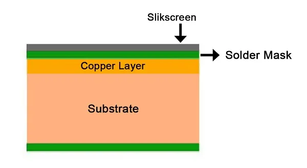
What Is Copper Foil Thickness and Why It Matters
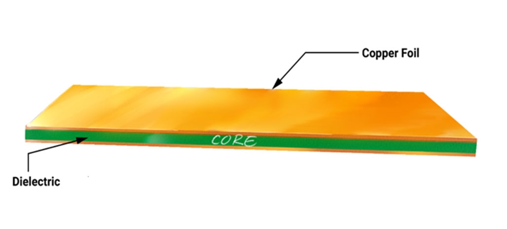
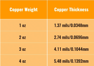
Copper foil thickness in PCBs refers to the amount of copper layered on the board’s surface, typically measured in ounces per square foot. This measurement indicates the weight of copper spread over a one square foot area, translating to a specific thickness. For instance, 1 ounce per square foot corresponds to approximately 1.4 mils or 35 micrometers. Copper serves as the conductive pathway for electrical signals and power in a circuit, making its thickness a key factor in performance.
Why does this matter for hobbyists? The copper weight affects current carrying capacity, heat dissipation, and the ease of etching during DIY PCB design. Thinner copper may be easier to etch at home but might not handle higher currents, risking overheating or damage. Thicker copper supports more current but can be challenging to work with in simple PCB projects. Understanding these trade-offs ensures your design meets functional needs without unnecessary complexity.
Related Reading: Practical Advantages of High-Tensile, High-Ductility Copper Foil
Technical Principles Behind Copper Thickness
Copper thickness in PCBs is not just about the physical layer but also about electrical and thermal behavior. The primary principle is current carrying capacity, which is governed by the cross sectional area of the copper trace. Thicker copper provides a larger area, reducing resistance and allowing more current to flow without excessive heat buildup. Standards like IPC 2221B, which provides guidelines for PCB design, include tables for determining trace width and thickness based on current requirements.
Another key factor is thermal management. Copper acts as a heat sink, dissipating heat generated by components. Thicker layers spread heat more effectively, protecting sensitive parts in your circuit. Additionally, copper weight impacts signal integrity, especially in high speed designs, though this is less critical for most hobbyist projects. For DIY enthusiasts etching PCBs at home, thinner copper is often preferred due to easier chemical removal during the etching process.
Choosing the Right Copper Weight for Hobby PCBs
Selecting the appropriate copper weight for hobby PCBs depends on your project’s requirements and fabrication method. Here are the common copper weights and their applications for hobbyists.
- 0.5 ounce per square foot (17.5 micrometers): This is the thinnest standard copper layer, suitable for low current, simple PCB projects. It is easy to etch at home but limited in current capacity.
- 1 ounce per square foot (35 micrometers): The most common choice for hobbyists and general purpose designs. It balances ease of etching with adequate current handling for most DIY circuits.
- 2 ounces per square foot (70 micrometers): Used for higher current applications, such as power supplies. It is harder to etch manually and may require more robust tools.
For most hobbyists engaging in DIY PCB design, 1 ounce copper is a safe starting point. It supports typical current levels in small projects while being manageable during home etching. If your project involves high power components, consider 2 ounces, but be prepared for additional effort in processing. Always calculate the expected current using guidelines from standards like IPC 2221B to ensure safety.
Practical Tips for DIY PCB Design and Etching at Home
Creating PCBs at home is a rewarding process for hobbyists, but it requires attention to detail, especially when dealing with copper foil. Here are actionable tips to help you succeed in etching PCBs at home while considering copper thickness.
First, choose a suitable copper clad board based on your project needs. For beginners, start with 1 ounce copper on a single sided board. This thickness is forgiving during etching and widely available. Ensure your workspace is well ventilated, as etching chemicals release fumes.
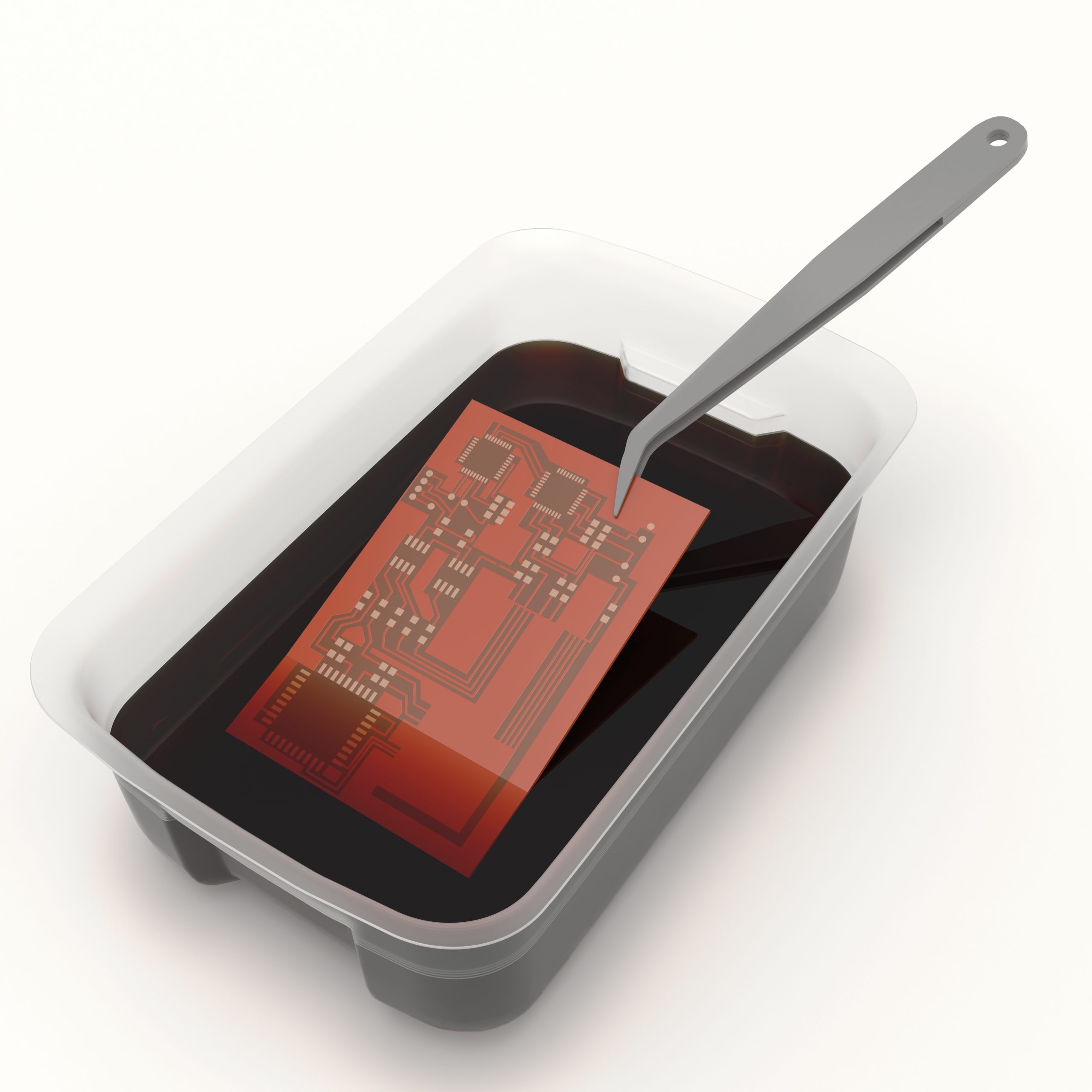
Next, design your circuit layout using free software tools that allow you to specify trace widths based on current needs. Print your design onto a transfer medium, such as toner transfer paper, and apply it to the copper clad board. During etching, use a solution like ferric chloride or a mixture of hydrochloric acid and hydrogen peroxide. Thinner copper etches faster, reducing exposure time and minimizing undercutting of traces.
Finally, inspect your board after etching. Use a multimeter to check for continuity and ensure no copper remains where it should not be. If traces are too thin due to over etching, consider wider traces in future designs or switch to a thicker copper weight for durability.
Related Reading: Step by Step: Creating Inner Layers Using Home Etching Methods
Simple PCB Projects to Practice Copper Thickness Selection
For hobbyists new to PCB design, starting with simple PCB projects helps build confidence in selecting copper weights and etching techniques. Here are three beginner friendly ideas to try.
- LED Blinking Circuit: This project uses a basic microcontroller or timer IC to blink LEDs. A 1 ounce copper board is ideal, as the current draw is minimal. Focus on clean trace layouts to avoid shorts during etching at home.
- Simple Power Supply: Build a regulated 5 volt supply for other projects. Depending on the output current, you might need 1 or 2 ounce copper. Calculate trace widths using IPC 2221B guidelines to prevent overheating.
- Audio Amplifier: A small amplifier circuit for headphones or speakers is a step up in complexity. Use 1 ounce copper for low power designs, ensuring traces can handle the amplifier’s current without excessive resistance.
Common Challenges and Troubleshooting in Home PCB Fabrication
Even with careful planning, hobbyists often face challenges when working with copper foil and etching PCBs at home. One common issue is uneven etching, where some areas of copper remain due to insufficient chemical action. This can be mitigated by agitating the etching solution regularly and ensuring the board is fully submerged. If using a thinner copper weight, reduce etching time to avoid over removal.
Another challenge is trace breakage, especially with thinner copper like 0.5 ounce. Narrow traces can lift or break during handling. To prevent this, design wider traces where possible, and handle the board gently after etching. If breakage occurs, small repairs can be made with conductive ink or thin wire.
Lastly, achieving consistent results with thicker copper, such as 2 ounces, is difficult in a home setup. The etching process takes longer, increasing the risk of undercutting. For such projects, consider professional fabrication if the design exceeds your equipment’s capability.
Conclusion
Understanding copper foil thickness is a cornerstone of successful PCB design for electronic hobbyists. By grasping the principles of copper weight for hobby PCBs, you can make informed decisions that balance performance and ease of fabrication. Whether you are etching a PCB at home or designing a simple circuit, starting with a standard 1 ounce copper layer offers versatility for most projects. As you grow in skill, experimenting with different thicknesses will enhance your ability to tackle complex designs. Use this guide as a foundation to explore the exciting world of DIY PCB design, ensuring your creations are both functional and reliable.
FAQs
Q1: What is the best copper weight for hobby PCBs in simple projects?
A1: For most simple PCB projects, a copper weight of 1 ounce per square foot is ideal. It provides a good balance between current carrying capacity and ease of etching at home. This thickness suits low to moderate current needs and is manageable for beginners using basic tools and chemicals, ensuring successful DIY PCB design without excessive complexity.
Q2: How does PCB copper thickness affect etching at home?
A2: PCB copper thickness significantly impacts the etching process during home fabrication. Thinner copper, like 0.5 or 1 ounce, etches faster and requires less time in chemical solutions, reducing the risk of over etching. Thicker copper, such as 2 ounces, takes longer and may lead to uneven results without proper agitation, making it more challenging for hobbyists.
Q3: What are some beginner tips for DIY PCB design with copper foil?
A3: Start with a 1 ounce copper clad board for ease of handling in DIY PCB design. Use free design software to plan trace widths based on current needs. During etching, work in a ventilated area, and monitor the process closely to avoid over removal. Finally, test your board with a multimeter to confirm connectivity after etching.
Q4: How do I choose copper thickness for high current simple PCB projects?
A4: For high current simple PCB projects, consider a copper weight of 2 ounces per square foot to handle increased power without overheating. Use guidelines from standards like IPC 2221B to calculate trace widths. While etching thicker copper at home is harder, it ensures safety and reliability for power intensive hobbyist designs.
References
IPC 2221B: Generic Standard on Printed Board Design. IPC, 2012.
IPC-A-600K: Acceptability of Printed Boards. IPC, 2020.