Introduction
The demand for miniaturization and geometric versatility in modern electronics has pushed traditional rigid circuit boards to their physical limits. As industries ranging from aerospace to medical devices require lighter, smaller, and more reliable interconnects, engineers are increasingly turning to flexible and rigid-flex technologies. However, transitioning from rigid to flexible substrates introduces a new dimension of complexity that spans mechanical engineering, material science, and manufacturing logistics.
This guide serves as a central resource for understanding the holistic process of designing and manufacturing flexible circuits. It moves beyond isolated design rules to establish a cohesive framework. We will address how to manage complex stack-ups, navigate unique schematic requirements, and implement design-for-assembly (DFA) protocols that prevent costly failures on the production floor. The goal is to equip technical decision-makers with the knowledge to integrate electrical performance with mechanical endurance seamlessly.
Core Concepts and Overall Framework
Before diving into specific design strategies, it is essential to define the architectural differences that separate these technologies from standard PCBs.
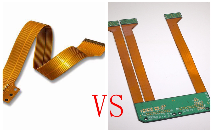
Flexible PCBs are standalone circuits built on flexible polymer films, allowing them to bend or twist to fit into confined spaces. Rigid-Flex PCBs are hybrid structures where flexible circuit layers are physically laminated into rigid board sections. This allows for a continuous electrical connection that eliminates the need for heavy, bulky connectors.
The design process for these boards requires a shift in mindset. Unlike rigid boards where the substrate is a static platform, the substrate in flex circuits is an active mechanical component. Engineers must consider the Bend Radius (the minimum limit a board can flex without damage) and the Neutral Axis (the layer where minimal stress occurs during bending). Successful implementation relies on managing the interplay between these mechanical constraints and electrical requirements throughout the fabrication lifecycle.
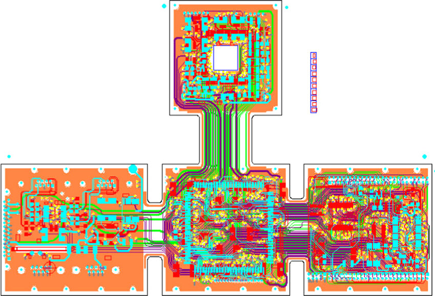
Flex and Rigid Flex Multi Layer PCBs Design
As device functionality increases, the need for higher density routing often necessitates moving beyond single or double-sided flex circuits into complex multi-layer structures.
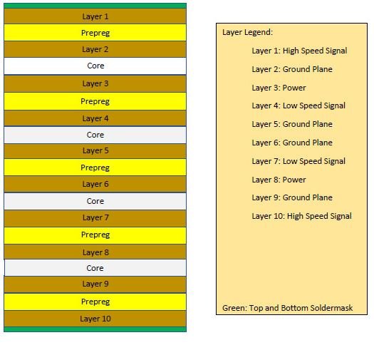
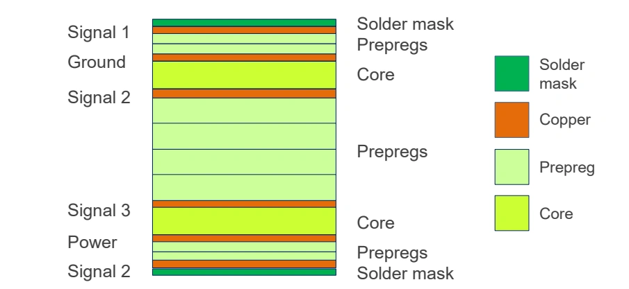
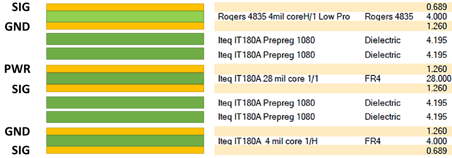
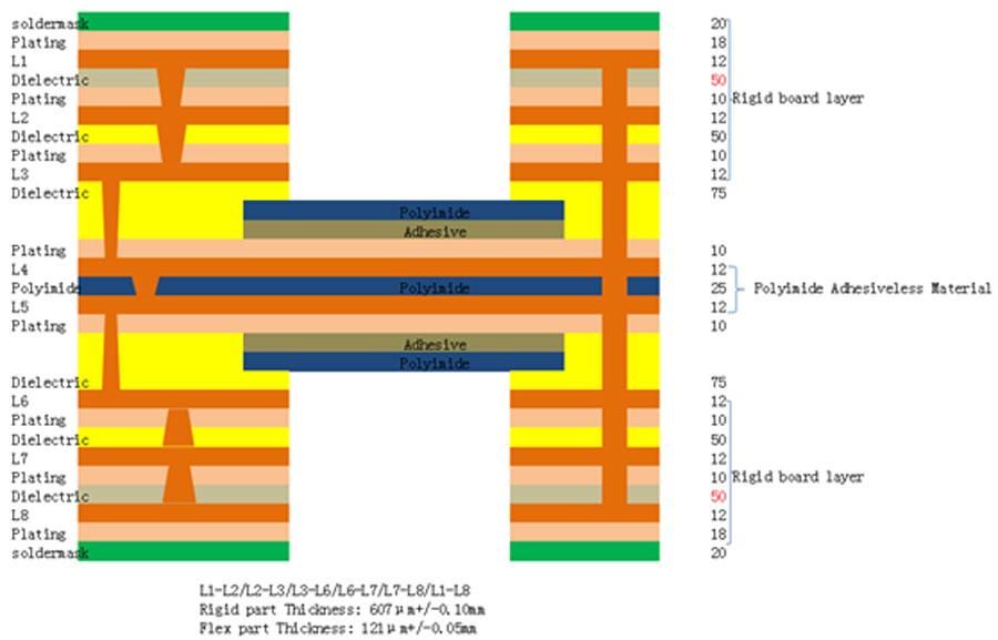
Scaling up the layer count in flexible designs introduces significant challenges regarding Z-axis expansion and registration, requiring a meticulous approach to material selection. When developing multi-layer flex and rigid-flex designs, engineers must account for the high coefficient of thermal expansion (CTE) inherent in acrylic adhesives. If not managed correctly, the thermal stress during reflow soldering can cause plated through-holes (PTH) to crack. To mitigate this, many high-reliability applications now favor adhesiveless laminates. These materials offer thinner profiles and better thermal stability, though they require precise processing parameters to ensure layer-to-layer alignment remains within tolerance.
PCB Schematic Design for Flex and Rigid Flex Circuits
The logical representation of a circuit must evolve to reflect the physical reality of a board that occupies three-dimensional space.
Standard schematic capture tools often treat a PCB as a single flat entity, but rigid-flex designs require a more nuanced approach where the schematic dictates distinct mechanical zones. Addressing pcb schematic design challenges involves assigning components to specific rigid or flex layers early in the logical design phase. This practice prevents the accidental placement of critical components in bend areas and ensures that the netlist reflects the unique impedance requirements of signals traveling across different substrate materials. By defining layer stacks and zones within the schematic software, designers can visualize the signal path's physical journey before a single trace is routed.
Implementing DFA in Flex and Rigid Flex PCB Design
A design that passes electrical simulation is only valuable if it can be assembled reliably without damaging the fragile flexible substrate.
Because flexible materials are inherently unstable and prone to movement during processing, standard assembly line assumptions often lead to manufacturing defects. rigorous application of dfa in flex pcb design is critical for maintaining high yield rates. This includes adding tooling holes for negative retention, designing breakaway tabs that support the flex areas during conveyor transport, and ensuring sufficient clearance between solder pads and the coverlay interface. Furthermore, DFA protocols dictate that heavy components must be placed on the rigid sections or stiffened areas to prevent solder joint fatigue caused by mechanical vibration or handling during final integration.
The Structural Role of Copper Balancing
While often viewed as an electrical concern for signal return paths, copper distribution plays a primary mechanical role in flexible circuit fabrication.
Uneven distribution of copper across the layers of a flexible board creates internal stress that manifests as warpage or twisting after etching and lamination. Implementing strategic copper balancing in flex pcbs ensures that the board remains flat and dimensionally stable. This involves using cross-hatched copper pours rather than solid planes in flexible areas to retain pliability while providing electromagnetic shielding. By balancing the metal load on the top and bottom layers, manufacturers can prevent the "bimetallic strip effect" where the substrate curls during thermal cycling, ensuring the board fits correctly into assembly fixtures.
Step Up Stencil Solutions for Flex and Rigid Flex PCBs
The final hurdle in the manufacturing process is ensuring reliable solder paste deposition on a surface that may not be perfectly flat.
The interface between the rigid and flexible sections often creates slight height variations that standard stencils cannot accommodate effectively. To solve this, assembly houses utilize step-up stencil solutions which feature relieved areas on the squeegee side. These specialized tools allow the stencil to sit flush against the rigid sections while accommodating the slightly elevated or depressed flexible zones or stiffeners. Achieving the correct volume of solder paste is vital because flex circuits are less forgiving of rework; excessive heat from manual soldering irons can easily delaminate the pads from the base polyimide.
The Symbiosis of Electrical and Mechanical Constraints
The subtopics outlined above demonstrate that flexible circuit design is an exercise in compromise and optimization. A decision made in the schematic phase regarding component groups dictates the layer stack-up. This stack-up determines the necessary copper balancing strategy, which in turn influences the flatness of the board for stencil printing.
For instance, if a designer ignores copper balancing to maximize current carrying capacity, the resulting bow in the board may make automated assembly impossible, rendering the DFA efforts moot. Successful engineering teams treat these elements not as sequential steps but as a circular feedback loop where mechanical behavior is simulated alongside electrical performance.
Industry Considerations for Reliability and Yield
From a manufacturing and quality assurance perspective, the transition to flex and rigid-flex represents a significant investment in reliability. While the initial tooling and fabrication costs are higher than rigid PCBs, the reduction in assembly points and weight offers long-term value.
However, the margin for error is slim. In industries such as automotive and defense, the reliability of the interconnect is paramount. This requires strict adherence to inspection standards like IPC-6013. Engineers must prioritize the use of teardrops on pads to prevent cracking and specify flexible solder masks that can endure dynamic movement. Ultimately, the industry creates robust products by acknowledging that the flexible circuit is a mechanical actuator as much as it is an electrical conduit.
Conclusion
Designing and manufacturing Flex and Rigid-Flex PCBs requires a sophisticated synthesis of logic, physics, and process engineering. It is not enough to simply route traces on a different material; one must architect a system that withstands thermal stress, mechanical bending, and rigorous assembly challenges.
By mastering multi-layer stack-up configurations, integrating mechanical constraints into schematics, and adhering to strict DFA and copper balancing rules, engineers can unlock the full potential of this technology. As the electronics industry continues to favor compact and integrated designs, the ability to execute these complex fabrications with high yield and reliability will distinguish market-leading products from the rest. This framework provides the essential roadmap for navigating that complexity with confidence.