Introduction
Power integrity is a cornerstone of modern printed circuit board (PCB) design, ensuring that electronic devices operate reliably under varying conditions. For electrical engineers, achieving robust power integrity in PCB construction is critical to prevent issues like voltage drops, noise, and signal degradation. A well designed power distribution network (PDN) directly impacts system performance, especially in high speed and high power applications. This article explores essential strategies for power integrity in PCB construction, focusing on PDN design, decoupling capacitor placement, and power plane design. By integrating power integrity simulation into the workflow, engineers can anticipate and mitigate potential challenges. Aimed at professionals in the field, this guide offers practical insights and best practices aligned with industry standards to optimize PCB performance and reliability.
What Is Power Integrity and Why It Matters
Power integrity refers to the ability of a PCB to deliver stable and clean power to all components across a range of operating frequencies and conditions. It ensures that voltage levels remain within specified tolerances, minimizing noise and transients that can disrupt circuit functionality. In high speed digital systems, poor power integrity can lead to signal integrity issues, increased electromagnetic interference (EMI), and system failures. For engineers, maintaining power integrity in PCB construction is vital as it directly affects product reliability and performance. With the rise of compact, high density designs, the challenge of managing power distribution becomes even more pronounced. A robust PDN design in PCB construction is essential to support the increasing demands of modern electronics, from consumer gadgets to industrial systems.
Technical Principles of Power Integrity in PCB Design
Power integrity hinges on managing the impedance of the power distribution network to ensure minimal voltage fluctuations. The PDN must supply adequate current to components while suppressing noise across a wide frequency spectrum. Key factors influencing power integrity include parasitic inductance, resistance in power paths, and the effectiveness of decoupling mechanisms. High frequency switching in digital circuits can cause rapid current changes, leading to voltage drops if the PDN impedance is not controlled. Power plane design plays a crucial role in reducing inductance by providing low impedance paths for current flow. Additionally, improper decoupling capacitor placement can fail to suppress noise, exacerbating power integrity issues. Understanding these principles allows engineers to anticipate challenges and design PCBs that maintain stable power delivery under dynamic conditions.
Key Strategies for Power Integrity in PCB Construction
Optimizing PDN Design in PCB Construction
A well structured power distribution network is the backbone of power integrity in PCB construction. Engineers should prioritize low impedance paths to minimize voltage drops during transient events. This involves using wide traces or dedicated power planes to reduce resistance and inductance. Splitting power planes into isolated sections for different voltage domains can prevent noise coupling between sensitive circuits. Adhering to guidelines such as those in widely recognized industry standards ensures that PDN design meets performance expectations. Simulations during the design phase help identify potential weaknesses in the network, allowing for adjustments before fabrication. A robust PDN design in PCB construction also considers current density to avoid overheating and ensure long term reliability of the board.
Suggested Reading: Mastering PDN Impedance: Key to Robust PCB Power Integrity
Effective Decoupling Capacitor Placement
Decoupling capacitors are essential for maintaining power integrity by filtering high frequency noise and providing local charge storage. Their placement is critical to effectiveness. Capacitors should be positioned as close as possible to the power pins of integrated circuits to minimize loop inductance. Using a range of capacitor values addresses noise across different frequency bands, from low to high. Vias connecting capacitors to power and ground planes must be optimized to reduce parasitic effects. Engineers should also consider the physical layout to avoid clustering capacitors in areas prone to interference. Proper decoupling capacitor placement enhances the stability of the power supply, reducing the risk of voltage fluctuations that could impair device operation.
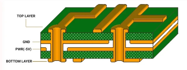
PCB Power Plane Design for Low Impedance
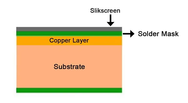
Power plane design is a fundamental aspect of achieving power integrity in PCB construction. Solid power and ground planes in multilayer boards create a low impedance path for current, reducing voltage noise. Placing power and ground planes adjacent to each other forms a natural capacitance, aiding in high frequency noise suppression. Engineers should avoid splitting planes unnecessarily, as gaps can increase inductance and disrupt current flow. When splits are required for multiple voltage levels, careful planning ensures minimal impact on impedance. Stitching vias around plane edges can further improve return path continuity. A well executed PCB power plane design supports stable power delivery, essential for high performance systems.
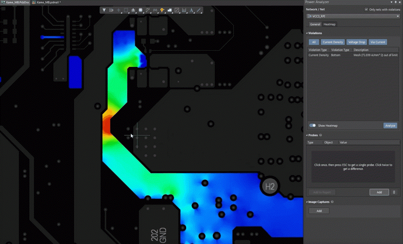
Leveraging Power Integrity Simulation
Power integrity simulation is a powerful tool for identifying and resolving potential issues before quick turn PCB fabrication. It allows engineers to model the PDN and analyze impedance profiles across frequencies. Simulations can reveal areas of high voltage drop or excessive noise, guiding adjustments in layout or component selection. Tools aligned with industry practices enable accurate prediction of transient responses and capacitor effectiveness. By incorporating power integrity simulation early in the design process, engineers can optimize decoupling capacitor placement and power plane configurations. This proactive approach reduces costly redesigns and ensures the PCB meets performance requirements under real world conditions.
Best Practices for Implementing Power Integrity Strategies
To achieve optimal power integrity in PCB construction, engineers should follow several best practices. First, prioritize a multilayer stackup with dedicated power and ground planes to minimize impedance. Second, use multiple decoupling capacitors with varied values near critical components to cover a broad frequency range. Third, ensure short, direct connections between components and power planes using vias strategically placed to reduce inductance. Fourth, validate designs with power integrity simulation to identify potential issues before manufacturing. Finally, adhere to established standards like IPC-6012E for rigid board performance to ensure consistent quality. These practices collectively enhance the reliability of the power distribution network, supporting robust operation in demanding applications.
Troubleshooting Common Power Integrity Issues
Power integrity issues often manifest as erratic behavior in circuits, such as unexpected resets or data corruption. One common problem is excessive noise due to inadequate decoupling capacitor placement. Engineers can address this by reviewing capacitor positions and adding more if necessary near high current components. Another issue is voltage drop caused by high PDN impedance, often resolved by widening traces or optimizing power plane design. Ground bounce, resulting from poor return paths, can be mitigated by ensuring continuous ground planes and strategic via placement. Using power integrity simulation during troubleshooting helps pinpoint the root cause of issues, enabling targeted fixes. Regular design reviews against standards like IPC-A-600K ensure that potential problems are caught early in the process.
Conclusion
Designing PCBs with power integrity in mind is essential for ensuring reliable performance in modern electronic systems. By focusing on PDN design in PCB construction, optimizing decoupling capacitor placement, and implementing effective PCB power plane design, engineers can mitigate noise and voltage fluctuations. Power integrity simulation serves as a critical tool for validating designs and identifying issues before they impact functionality. Adhering to industry standards and best practices further enhances the quality and durability of PCBs. For electrical engineers, mastering these strategies is key to meeting the demands of high speed and high power applications, ultimately delivering robust and efficient designs.
FAQs
Q1: How does PDN design in PCB construction affect power integrity?
A1: PDN design in PCB construction is crucial for maintaining power integrity by ensuring low impedance paths for current delivery. A well designed PDN minimizes voltage drops and noise during transient events, supporting stable operation. Engineers must optimize trace widths and plane layouts to handle current demands. Following industry standards helps achieve reliable power distribution across the board.
Q2: What are the key factors in effective decoupling capacitor placement?
A2: Decoupling capacitor placement is vital for filtering noise and stabilizing voltage near components. Place capacitors close to power pins to reduce loop inductance and use varied values for different frequency ranges. Minimize via lengths to connect to planes effectively. Proper placement ensures quick charge delivery, preventing power integrity issues in high speed circuits.
Q3: Why is PCB power plane design important for system reliability?
A3: PCB power plane design directly impacts system reliability by providing low impedance paths for current flow. Adjacent power and ground planes create capacitance, suppressing high frequency noise. Avoiding unnecessary splits and using stitching vias maintains continuity. A solid plane design reduces voltage fluctuations, ensuring consistent performance in demanding applications.
Q4: How can power integrity simulation improve PCB design outcomes?
A4: Power integrity simulation helps engineers model PDN behavior and analyze impedance across frequencies. It identifies potential voltage drops and noise issues before fabrication, allowing for layout adjustments. Simulating decoupling capacitor effectiveness and plane configurations optimizes designs. This approach reduces redesign costs and ensures PCBs meet performance expectations in real world conditions.
References
IPC-6012E — Qualification and Performance Specification for Rigid Printed Boards. IPC, 2020.
IPC-A-600K — Acceptability of Printed Boards. IPC, 2020.