Introduction
For electronic hobbyists, crafting custom printed circuit boards (PCBs) at home opens up a world of possibilities. One exciting project is building a DIY PCB signal booster to enhance communication signals for devices like cell phones or radios. A critical aspect of such projects is controlled depth drilling, which ensures precision when creating vias or mounting components without damaging the board. This guide explores how hobbyists can achieve controlled depth drilling at home and build a signal booster using basic tools and techniques. By focusing on PCB project ideas and improving signal strength, this article provides practical steps tailored for enthusiasts eager to elevate their electronics skills with hands-on solutions.
What Is a DIY PCB Signal Booster and Why It Matters
A DIY PCB signal booster is a custom circuit designed to amplify weak signals, often for wireless communication devices. Hobbyists might use it to improve reception in areas with poor coverage or to enhance the performance of homemade radios. The relevance of such a project lies in its ability to solve real-world problems with minimal cost while offering a deep learning experience in electronics.
Signal boosters typically work by capturing weak signals through an antenna, amplifying them using active components like transistors or operational amplifiers, and retransmitting the enhanced signal. For hobbyists, building one on a fast turn custom PCB not only teaches circuit design but also introduces fabrication challenges like precise drilling. Improving signal strength on a PCB is vital, as poor design or construction can lead to noise or signal loss, defeating the purpose of the booster.
Technical Principles of Signal Boosters and PCB Drilling
How Signal Boosters Function
At its core, a signal booster relies on amplification. The input signal, often faint, passes through a circuit that increases its amplitude without distorting the original information. Common designs for hobbyist electronics use low-noise amplifiers to minimize interference. The PCB layout plays a crucial role here. Traces must be short to avoid parasitic capacitance, and ground planes should be used to reduce electromagnetic interference.
The choice of components also affects performance. For instance, selecting a transistor with appropriate gain and frequency response ensures the booster operates within the desired range. Additionally, impedance matching between the antenna, amplifier, and output is necessary to maximize power transfer and prevent signal reflection.
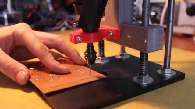
Controlled Depth Drilling Explained
Controlled depth drilling refers to the process of drilling holes in a PCB to a specific depth without penetrating through the entire board or damaging underlying layers. This technique is essential for multilayer boards or when creating blind vias, which connect only certain layers. For a DIY PCB signal booster, precise drilling ensures components are mounted correctly and vias maintain signal integrity.
The principle behind controlled depth drilling is simple yet requires care. A drill bit is lowered to a predetermined depth, often guided by a stop mechanism or manual adjustment. In professional settings, machines use laser or mechanical sensors for accuracy. At home, hobbyists can adapt by using drill presses with depth stops or even hand drills with marked bits. The challenge lies in maintaining consistency across multiple holes while avoiding board damage.
Challenges in DIY PCB Fabrication for Signal Boosters
Creating a PCB at home for a signal booster involves several hurdles. First, ensuring signal strength requires careful trace design to avoid crosstalk or loss. High-frequency signals, common in communication devices, are particularly sensitive to layout flaws. Second, drilling precision is critical. A misaligned or overly deep hole can sever traces or weaken the board structure.
Another concern is material selection. Most hobbyists use FR-4, a standard glass-reinforced epoxy laminate, for its affordability and availability. However, its dielectric properties may not always be ideal for high-frequency applications. Understanding these limitations helps in designing a functional booster despite the constraints of home fabrication.
Practical Solutions for Controlled Depth Drilling at Home
Tools and Setup for Hobbyists
Achieving controlled depth drilling at home does not require expensive equipment. A basic drill press with an adjustable depth stop is ideal, as it allows consistent drilling depth. For those without a drill press, a handheld drill can work if paired with a simple depth guide, such as a piece of tape wrapped around the bit to mark the desired depth.
Here are essential tools for hobbyists:
- Drill press or handheld drill
- Small drill bits (0.8 mm to 1.2 mm for typical vias)
- Depth stop or marking tape
- PCB material (single or double-sided FR-4)
- Safety gear like goggles and gloves
Before starting, secure the PCB on a flat, stable surface using a vice or clamps. This prevents movement during drilling, which could lead to inaccurate holes. Always test the depth setting on a scrap piece of material to confirm accuracy.

Step-by-Step Guide to Controlled Depth Drilling
- Mark the drilling locations on the PCB using a fine-tip marker or layout software printout.
- Set the depth stop on the drill press to the desired depth, typically just enough to penetrate the top layer for blind vias.
- Align the drill bit over the marked spot and lower it slowly to avoid splintering the board.
- Drill at a steady speed, applying minimal pressure to prevent overheating or bit breakage.
- Clean the board with a brush to remove debris after drilling each hole.
For multilayer boards, measure the layer thickness to ensure the drill does not reach underlying traces. If using a handheld drill, practice on scrap boards to develop a feel for the depth.
Tips for Improving Signal Strength on PCB
While drilling is crucial, the overall design impacts the booster’s performance. Use a ground plane to shield signals from interference. Keep high-frequency traces short and direct to minimize loss. Place decoupling capacitors near active components to stabilize power supply and reduce noise. These practices, grounded in basic electrical engineering principles, ensure the PCB supports the booster’s goal of amplifying signals effectively.
Suggested Reading: Controlled Depth Drilling for Beginners: A Hobbyist's Guide to PCB Perfection
Building Your DIY PCB Signal Booster
Designing the Circuit
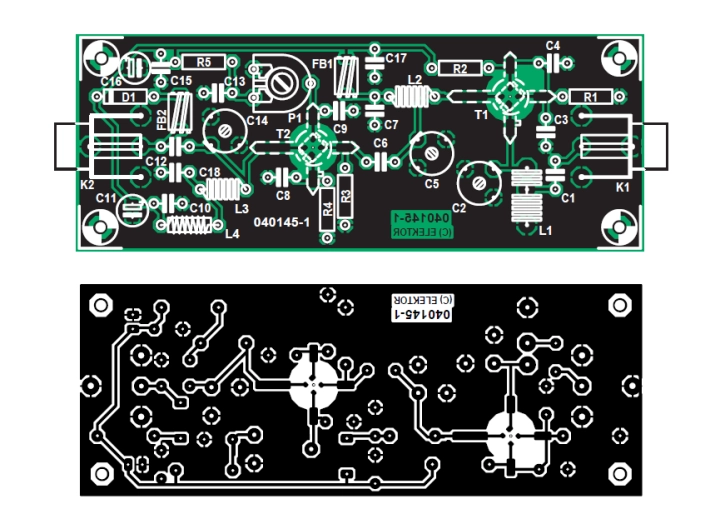
Start with a simple amplifier circuit suitable for hobbyist electronics. A common choice is a single-stage transistor amplifier, which can boost signals in a specific frequency range. Use free schematic capture tools to draw the circuit, ensuring all components are placed logically. Transfer the design to a PCB layout, prioritizing short traces for high-frequency signals.
Key components include:
- Transistor or operational amplifier for gain
- Resistors and capacitors for biasing and filtering
- Antenna for signal input and output
- Power supply (battery or DC source)
Fabricating the PCB at Home
Once the design is ready, etch the PCB using the toner transfer or photoresist method. Both are accessible to hobbyists and involve transferring the layout onto the copper-clad board before etching away excess copper with a chemical solution. After etching, drill holes for components and vias using the controlled depth technique described earlier.
Assembly and Testing
Solder components onto the board, starting with smaller parts like resistors and capacitors before moving to larger ones like transistors. Double-check connections to avoid shorts. Test the booster by connecting it to a signal source and measuring output with a multimeter or oscilloscope if available. Adjust component values if the gain is insufficient or noise is high.
Troubleshooting Common Issues in DIY Signal Boosters
Hobbyists often face issues like low gain or excessive noise. If the booster fails to amplify, check for soldering errors or incorrect component values. Noise can stem from poor grounding or long traces acting as antennas for interference. Adding a ground plane or shielding sensitive areas with copper foil can help. For drilling errors, such as holes that are too deep, use conductive epoxy to repair damaged traces, though prevention through practice is better.
Conclusion
Building a DIY PCB signal booster is a rewarding project for electronic hobbyists, combining circuit design with hands-on fabrication skills. Controlled depth drilling at home, while challenging, becomes manageable with the right tools and techniques. By focusing on precision and following best practices for improving signal strength on a PCB, enthusiasts can create functional devices that rival commercial solutions. This guide offers a foundation for such PCB project ideas, empowering hobbyists to experiment and innovate in their home workshops.
FAQs
Q1: What tools are essential for controlled depth drilling at home?
A1: For controlled depth drilling at home, hobbyists need a drill press with a depth stop or a handheld drill with a marked bit. Small drill bits (0.8 mm to 1.2 mm) are necessary for vias. A stable work surface, clamps, and safety gear like goggles are also crucial to ensure precision and safety during the process.
Q2: How can I ensure improving signal strength on a PCB for my booster?
A2: Improving signal strength on a PCB requires a solid ground plane to reduce interference. Keep high-frequency traces short and direct. Place decoupling capacitors near active components to stabilize power. These steps, based on fundamental design principles, help minimize noise and maximize the booster’s effectiveness.
Q3: What are some beginner-friendly PCB project ideas related to signal boosters?
A3: Beginner-friendly PCB project ideas include designing a simple FM radio signal booster or a low-power Wi-Fi range extender. Start with single-layer boards to simplify fabrication. These projects teach basic amplification and PCB layout skills while offering practical results for hobbyist electronics enthusiasts.
Q4: Why is controlled depth drilling important for hobbyist electronics?
A4: Controlled depth drilling is vital in hobbyist electronics to create precise vias or mounting holes without damaging the PCB. Incorrect drilling can sever traces or weaken the board, affecting performance. For signal boosters, precision ensures reliable connections, maintaining signal integrity across the circuit.
References
IPC-6012E — Qualification and Performance Specification for Rigid Printed Boards. IPC, 2020.
IPC-A-600K — Acceptability of Printed Boards. IPC, 2020.


