Introduction
For electronic hobbyists, producing small batches of custom printed circuit boards often comes with high costs and long lead times when relying on professional services. DIY PCB panelization offers a practical solution by allowing you to combine multiple individual boards into a single larger panel, streamlining home PCB fabrication processes. This approach not only reduces material waste but also makes it easier to handle boards during etching, drilling, and soldering at home. Whether you are prototyping a new sensor project or building several identical controllers, understanding PCB panelization for hobbyists can save time and money. In this guide, we explore the fundamentals, techniques, and best practices tailored for low-cost PCB panelization in a home workshop. By the end, you will have the knowledge to create efficient panels that yield reliable results.
PCB panelization refers to the process of arranging multiple individual circuit boards onto a single carrier panel to facilitate batch production and handling. In a DIY context, this means designing and fabricating panels at home using basic tools and materials, ideal for hobbyists who produce one-off or small-run projects. Traditional single-board fabrication can lead to inefficiencies, such as excessive copper waste or misalignment during manual etching, but panelization optimizes the use of your photoresist sheets or etching tanks. For home PCB fabrication, it enables consistent processing across boards, reducing errors from handling tiny individual pieces. Moreover, low-cost PCB panelization democratizes access to professional-like results without shipping fees or minimum order quantities. Ultimately, it empowers hobbyists to iterate designs faster while maintaining quality control in their own space.
The relevance for electronic hobbyists lies in scalability and cost-effectiveness. A single panel might hold 4 to 16 boards, depending on size, cutting fabrication time by half or more through unified exposure and development steps. It also simplifies fixturing for drilling or milling with desktop CNC routers common in hobby shops. Without panelization, small boards risk damage from tweezers or tape, leading to scrapped parts. By adopting this method, you align your home workflow with industry practices, ensuring boards meet basic reliability standards before assembly.
What Is DIY PCB Panelization and Why It Matters for Hobbyists
PCB panelization refers to the process of arranging multiple individual circuit boards onto a single carrier panel to facilitate batch production and handling. In a DIY context, this means designing and fabricating panels at home using basic tools and materials, ideal for hobbyists who produce one-off or small-run projects. Traditional single-board fabrication can lead to inefficiencies, such as excessive copper waste or misalignment during manual etching, but panelization optimizes the use of your photoresist sheets or etching tanks. For home PCB fabrication, it enables consistent processing across boards, reducing errors from handling tiny individual pieces. Moreover, low-cost PCB panelization democratizes access to professional-like results without shipping fees or minimum order quantities. Ultimately, it empowers hobbyists to iterate designs faster while maintaining quality control in their own space.
The relevance for electronic hobbyists lies in scalability and cost-effectiveness. A single panel might hold 4 to 16 boards, depending on size, cutting fabrication time by half or more through unified exposure and development steps. It also simplifies fixturing for drilling or milling with desktop CNC routers common in hobby shops. Without panelization, small boards risk damage from tweezers or tape, leading to scrapped parts. By adopting this method, you align your home workflow with industry practices, ensuring boards meet basic reliability standards before assembly.
Technical Principles of PCB Panelization
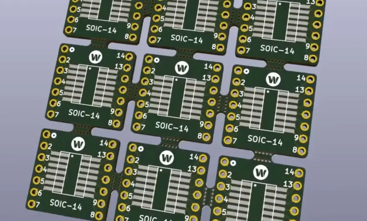
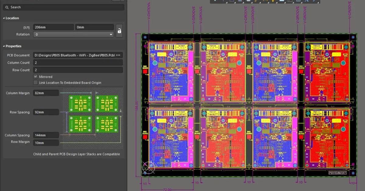
At its core, DIY PCB panelization involves strategic layout planning to ensure mechanical stability and ease of separation post-fabrication. Key elements include outer rails, breakaway tabs, and scoring lines that hold the panel together during processing but allow clean depanelization. Proper spacing between boards, typically 2 to 5 millimeters, prevents chemical bleed or thermal issues during soldering. Fiducial marks, small circular pads at panel corners, aid alignment for any automated steps like desktop pick-and-place, even in hobby setups. Material selection mirrors single-board choices, with FR-4 substrates providing the rigidity needed for flat panels up to 18 by 24 inches for home handling.
V-scoring and tab routing form the primary mechanisms for board separation. V-scoring creates angled grooves along the panel edges, following guidelines in IPC-2221B for printed board design, which recommends depths of one-third the board thickness for reliable breaks without delamination. Tab routing uses perforated mouse bites, small drilled holes connected by copper-free webs, offering flexibility for irregular shapes. These methods balance panel strength during fabrication with ease of manual depanelization using snips or a router. Warpage control is critical, as uneven copper distribution can bow the panel; symmetric layouts and balanced trace densities mitigate this per IPC-6012DS qualification specs for rigid boards. Understanding these principles ensures your panels survive home etching tanks and ovens intact.
Panel integrity also depends on tooling and registration features. Round fiducials with 1 millimeter diameter and clear zones prevent solder mask overprint, facilitating precise cuts. Rails, at least 5 millimeters wide, provide handling margins and mounting holes for jigs. Copper balancing prevents plating inconsistencies in DIY electroplating setups. Adhering to these technical aspects minimizes rejects and supports repeatability across projects.
Best Practices for Low-Cost PCB Panelization at Home
Start with design software to array your Gerber files into a panel, ensuring at least 10 millimeters from board edges to panel perimeter for stability. Orient boards identically to simplify processing, and include test coupons at panel edges for traceability, like trace width checks. For home PCB fabrication, limit panel size to your etching tank dimensions, typically under 12 by 12 inches to avoid uneven developer flow. Use 1.6 millimeter thick FR-4 for standard hobby stock, as it resists flexing during manual handling. Always simulate depanelization paths to avoid stressing components near edges.
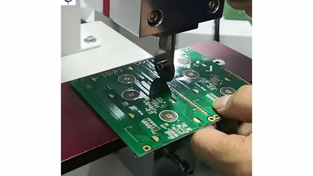
Depanelization techniques vary by method chosen during design. V-scored panels snap cleanly along the groove with a firm press on a straight edge, ideal for brittle separations without tools. Tab-routed panels require diagonal cutters for mouse bites, followed by sanding burrs smooth. For intricate shapes, a fine-tooth bandsaw or X-Y router with 0.8 millimeter end mills works well in hobby shops, using low RPM to prevent heat damage. Post-depanelization, inspect for microcracks under magnification, as per IPC-A-600K acceptability criteria for printed boards. These practices ensure functional boards ready for population.
Material and process optimization further enhances efficiency. Apply photoresist evenly across the full panel under yellow light to prevent premature exposure. During etching, agitate the solution vigorously for uniform copper removal, as panel size amplifies diffusion gradients. Bake panels at 100 degrees Celsius for 1 hour post-lamination to cure the resist fully. For multilayer hobby attempts, align inner layers precisely using registration pins. These steps make making PCB panels at home a reliable routine.
Safety and workspace setup cannot be overlooked. Secure panels in a vacuum jig for drilling to prevent bit wander, targeting 0.1 millimeter hole tolerances. Wear gloves and eye protection during chemical steps, and neutralize wastes properly. Store panels flat to avoid warpage from humidity. Document your panel yield per batch to refine future designs iteratively.
Common Challenges and Troubleshooting in DIY Panelization
Hobbyists often encounter warpage in larger panels due to asymmetric copper or improper storage. Balance trace areas across the panel and use conformal coating trials on test strips to verify flatness. If snapping V-scores causes cracks, reduce groove depth or add relief tabs. Misaligned fiducials from drilling shift can be fixed by recentering with a scribe before routing.
Another issue is tab remnants pulling traces during separation. Design tabs away from high-current paths and reinforce with ground pours. Etch undercuts from uneven exposure show as ragged edges; improve UV uniformity with a larger light source. For soldered panels, reflow warpage follows JEDEC J-STD-020E moisture sensitivity guidelines, so precondition boards dry. Troubleshooting systematically boosts success rates above 90 percent over time.
Conclusion
DIY PCB panelization transforms home PCB fabrication from a tedious task into an efficient workflow for electronic hobbyists. By mastering layout principles, separation methods, and best practices, you achieve low-cost PCB panelization with professional results. Key takeaways include balanced designs, standard-compliant features, and careful depanelization to minimize defects. Experiment iteratively, starting small, to build confidence. This approach not only cuts expenses but fosters deeper understanding of board production. Embrace PCB panelization for hobbyists to elevate your projects today.
FAQs
Q1: What is the easiest method for DIY PCB panelization at home?
A1: Tab routing with mouse bites suits beginners in home PCB fabrication, as it allows irregular board shapes and simple separation using cutters. Space holes 1 millimeter apart in 0.5 millimeter webs for clean breaks. This low-cost PCB panelization method avoids specialized tools, fitting most hobby workshops. Always sand edges post-cut to prevent shorts during assembly.
Q2: How much spacing is needed between boards in PCB panelization for hobbyists?
A2: Aim for 2 to 5 millimeters between boards to prevent etchant bleed and allow routing clearance in making PCB panels at home. This spacing supports manual handling without flex damage. Include 5 millimeter rails for grip. Adjust based on your desktop mill's collet size for precision.
Q3: Can V-scoring work for low-cost PCB panelization in DIY setups?
A3: Yes, V-scoring excels for rectangular boards in DIY PCB panelization, creating snap lines one-third board thickness deep per design standards. It requires no post-tools beyond sanding, ideal for hobbyists. Avoid on flexible substrates to prevent delamination. Test on scrap first for force needed.
Q4: What causes warpage in home-fabricated PCB panels?
A4: Uneven copper distribution or humidity exposure warps panels during PCB panelization for hobbyists. Balance layouts symmetrically and store flat in dry conditions. Bake pre-etch to relieve stresses. Inspect with a straightedge; mild cases flatten under weights.
References
IPC-2221B — Generic Standard on Printed Board Design. IPC, 2012
IPC-6012DS — Qualification and Performance Specification for Rigid Printed Boards. IPC, 2015
IPC-A-600K — Acceptability of Printed Boards. IPC, 2020
JEDEC J-STD-020E — Moisture/Reflow Sensitivity Classification of Nonhermetic Surface Mount Devices. JEDEC, 2014