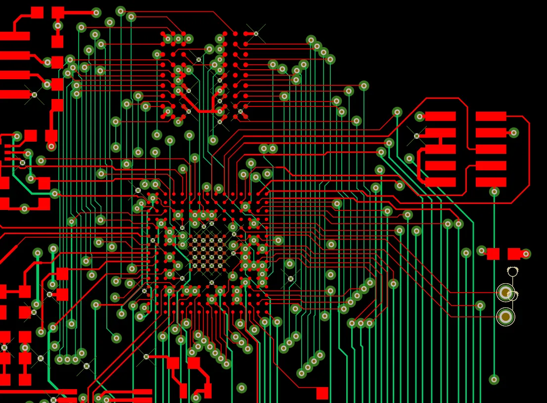
What Is a Solder Mask and Why Is It Essential for PCBs?
A solder mask serves as a crucial protective layer on a printed circuit board (PCB), designed primarily to prevent unintended solder bridges between closely spaced conductive traces. Beyond just preventing short circuits during soldering, this protective coating also acts as a shield, safeguarding the copper traces from environmental degradation such as oxidation, moisture, and dust. Its presence significantly contributes to the board's overall reliability and extended operational life.
Selecting the appropriate type of solder mask is a decision that impacts not only the PCB's functional performance but also influences the manufacturing workflow and the final production cost. The two predominant types in the industry are Dry Film Solder Mask and Liquid Photoimageable (LPI) Solder Mask. Each offers distinct characteristics that make them suitable for different applications, from high-precision electronics to general consumer devices.
How Does Dry Film Solder Mask Work?
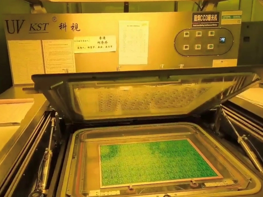
Dry Film Solder Mask is a sophisticated photosensitive polymer supplied in a solid sheet format, typically sandwiched between two release liners. During the PCB fabrication process, this film is carefully laminated onto the board's surface using a vacuum process, ensuring excellent adhesion and minimizing air bubbles. Subsequently, the laminated board is exposed to ultraviolet (UV) light through a photographic mask, which selectively cures the desired areas of the solder mask.
Following UV exposure, the board undergoes a development process where uncured sections of the film are washed away, revealing the copper pads where components will be soldered. The final step involves a thermal curing process, which fully hardens the remaining solder mask layer, ensuring its durability and resistance to various environmental stresses. This method is often favored for projects demanding exceptional precision and consistent thickness.
Key Benefits of Dry Film Solder Mask
Dry Film offers several compelling advantages, making it a preferred choice for specific applications:
● Consistent Thickness: This mask type provides a remarkably uniform layer thickness, typically ranging from 0.8 to 1.2 mils (20-30 microns). This consistency is vital for maintaining signal integrity in high-frequency designs, such as RF applications where impedance control is critical for optimal performance.
● Superior Precision: Dry Film is capable of achieving high resolution, accommodating fine-pitch components with trace widths and spacing as narrow as 3 mils (0.075 mm). This precision is indispensable for complex, densely populated PCB layouts.
● Enhanced Durability: The vacuum lamination process ensures robust adhesion to the PCB surface. This strong bond significantly reduces the risk of the mask peeling or cracking, even when subjected to thermal cycling or harsh operating conditions.
Potential Drawbacks of Dry Film Solder Mask
Despite its advantages, Dry Film Solder Mask also presents certain limitations:
● Higher Production Costs: The specialized materials, precise equipment required for vacuum lamination, and controlled exposure processes contribute to a higher overall cost. It can be 20-30% more expensive per square foot compared to other methods.
● Extended Processing Times: The multi-stage application process, including lamination, exposure, and development, can add an additional 1-2 hours per batch to the production timeline, potentially impacting projects with tight delivery schedules.
● Less Flexible for Irregular Designs: The film-based nature of Dry Film makes it less adaptable for boards with highly irregular shapes or designs that frequently undergo modifications. Precise cutting and application of the film are necessary, which can be challenging for non-standard geometries.
How Does Liquid Photoimageable (LPI) Solder Mask Operate?
Liquid Photoimageable (LPI) Solder Mask is a liquid ink that is applied directly to the PCB surface. This application is commonly performed using techniques such as silkscreening or spraying, ensuring even coverage across the board. Once applied, the liquid-coated board is exposed to ultraviolet (UV) light through a photolithographic film, which selectively cures the areas that will form the permanent solder mask.
After exposure, the unexposed, uncured portions of the liquid mask are washed away during a development stage, leaving behind openings for the solder pads. The final step involves a thermal or UV curing process to fully harden the remaining mask, ensuring its mechanical and chemical resistance. LPI is widely adopted across the electronics industry due to its versatility and cost-effectiveness, suitable for a broad spectrum of applications.
Advantages of Using LPI Solder Mask
LPI Solder Mask offers several compelling benefits that contribute to its widespread use:
● Economic Efficiency: LPI materials and their application methods are generally more affordable, often resulting in costs 20-30% lower per square foot than Dry Film. This makes LPI a highly attractive option for projects with budget constraints or high-volume consumer electronics manufacturing.
● Faster Turnaround: The application process for LPI, whether by spraying or silkscreening, is typically much quicker, often completed in under 30 minutes per batch. This efficiency can significantly accelerate production timelines.
● Versatile Application: LPI adapts easily to a wide array of board shapes and sizes, including irregular geometries. Its liquid form allows for seamless coverage, making it suitable for unique design requirements without the need for precise film cutting.
Limitations of LPI Solder Mask
Despite its benefits, LPI Solder Mask has certain drawbacks to consider:
● Variable Thickness: The thickness of LPI can fluctuate, typically ranging from 0.5 to 1.5 mils (12-38 microns), depending on the application technique. This inconsistency can affect impedance control in high-frequency designs, potentially leading to signal degradation or crosstalk at frequencies above 1 GHz.
● Reduced Precision for Fine Features: LPI is less suited for ultra-fine-pitch components, with resolution capabilities generally around 4-5 mils (0.1-0.125 mm). This limitation can pose challenges for extremely dense PCB designs requiring higher precision.
● Potential Durability Issues: Under conditions of extreme thermal stress or during multiple reflow cycles, LPI may be more susceptible to cracking or peeling, particularly if the curing process was not optimally performed.
Dry Film vs. LPI Solder Mask: A Comparative Overview
Choosing between Dry Film and LPI solder masks requires a thorough understanding of their core differences across various critical factors. This comparison helps in aligning the solder mask type with the specific demands of your PCB project.
Application and Thickness Characteristics
Dry Film involves the vacuum lamination of a solid film, ensuring a highly uniform thickness between 0.8 to 1.2 mils. This consistency is a significant advantage for designs where precise dielectric properties are paramount. In contrast, LPI is applied as a liquid ink via spraying or silkscreening, leading to more variable thickness, typically ranging from 0.5 to 1.5 mils. This variability can be a concern for high-frequency applications.
Precision and Production Efficiency
For designs requiring exceptional precision, especially with fine-pitch components, Dry Film excels, offering resolution down to 3 mils. This makes it ideal for densely packed or highly complex layouts. LPI provides moderate precision, generally around 4-5 mils, which is sufficient for most standard designs. In terms of processing time, Dry Film's multi-step lamination and development can take 1-2 hours per batch, while LPI's liquid application is faster, often under 30 minutes per batch.
Cost Implications and Best Use Cases
From a cost perspective, Dry Film is generally more expensive, often 20-30% higher per square foot due to specialized materials and equipment. LPI is typically 20-30% more economical, making it a popular choice for budget-conscious projects. Consequently, Dry Film is best suited for high-density, high-frequency, or mission-critical designs where precision and reliability are non-negotiable. LPI, with its lower cost and quicker application, is often preferred for standard designs, prototyping, and high-volume consumer electronics.
Which Solder Mask Type Aligns Best with Your PCB Project Needs?
The optimal choice between Dry Film and LPI Solder Mask ultimately depends on a careful evaluation of your PCB project's unique requirements, balancing performance, cost, and manufacturing considerations.
Prioritizing Precision and High-Frequency Performance
For projects demanding the highest level of precision, such as those involving fine-pitch components (with spacing below 4 mils) or operating at frequencies above 1 GHz, Dry Film is often the superior choice. Its uniform thickness and excellent resolution are critical for maintaining signal integrity in advanced applications like 5G communication boards, high-speed digital circuits, or complex medical electronics. Investing in Dry Film for these scenarios helps ensure the reliability and performance of sensitive designs.
Balancing Cost-Effectiveness with Standard Applications
If your project prioritizes budget-friendliness and involves standard designs without extreme precision requirements, LPI offers a practical and efficient solution. It's well-suited for consumer electronics, simple IoT devices, or LED lighting boards where cost is a significant factor and the performance needs are adequately met by LPI's capabilities. LPI is also an excellent option for prototyping or small production runs, thanks to its lower initial cost and faster processing times, allowing for more frequent design iterations without substantial financial overhead.
Considerations for Harsh Environments
For types of PCBs destined for harsh operating conditions, such as those in automotive or industrial control systems exposed to extreme temperatures, humidity, or aggressive chemicals, Dry Film's robust adhesion and superior durability might be a worthwhile investment. Its enhanced resistance to thermal shock and chemical exposure ensures long-term reliability in demanding environments, justifying the higher cost for critical applications.
Additional Factors to Consider When Selecting a Solder Mask
Beyond the primary distinctions, several other elements can influence the decision-making process for solder mask selection, affecting both functionality and aesthetics.
Environmental Compliance and Color Options
Both Dry Film and LPI solder masks are available in formulations that comply with international environmental standards, such as RoHS directives. Ensuring the chosen material meets all relevant regulatory requirements is essential for global market access. While green is the most common solder mask color, both types offer a variety of alternatives, including blue, red, and black. These non-green options might incur a slight additional cost (approximately $0.10-$0.20 per square foot) but are often selected for branding, aesthetic purposes, or to distinguish different board revisions.
Thermal and Chemical Resistance
Dry Film generally provides better resistance to thermal shock and chemical exposure compared to LPI. This enhanced resilience is particularly important for boards that will undergo multiple reflow soldering cycles or be subjected to aggressive cleaning agents during assembly or repair. The superior protective qualities of Dry Film contribute to the long-term integrity and performance of PCBs in challenging operational conditions.
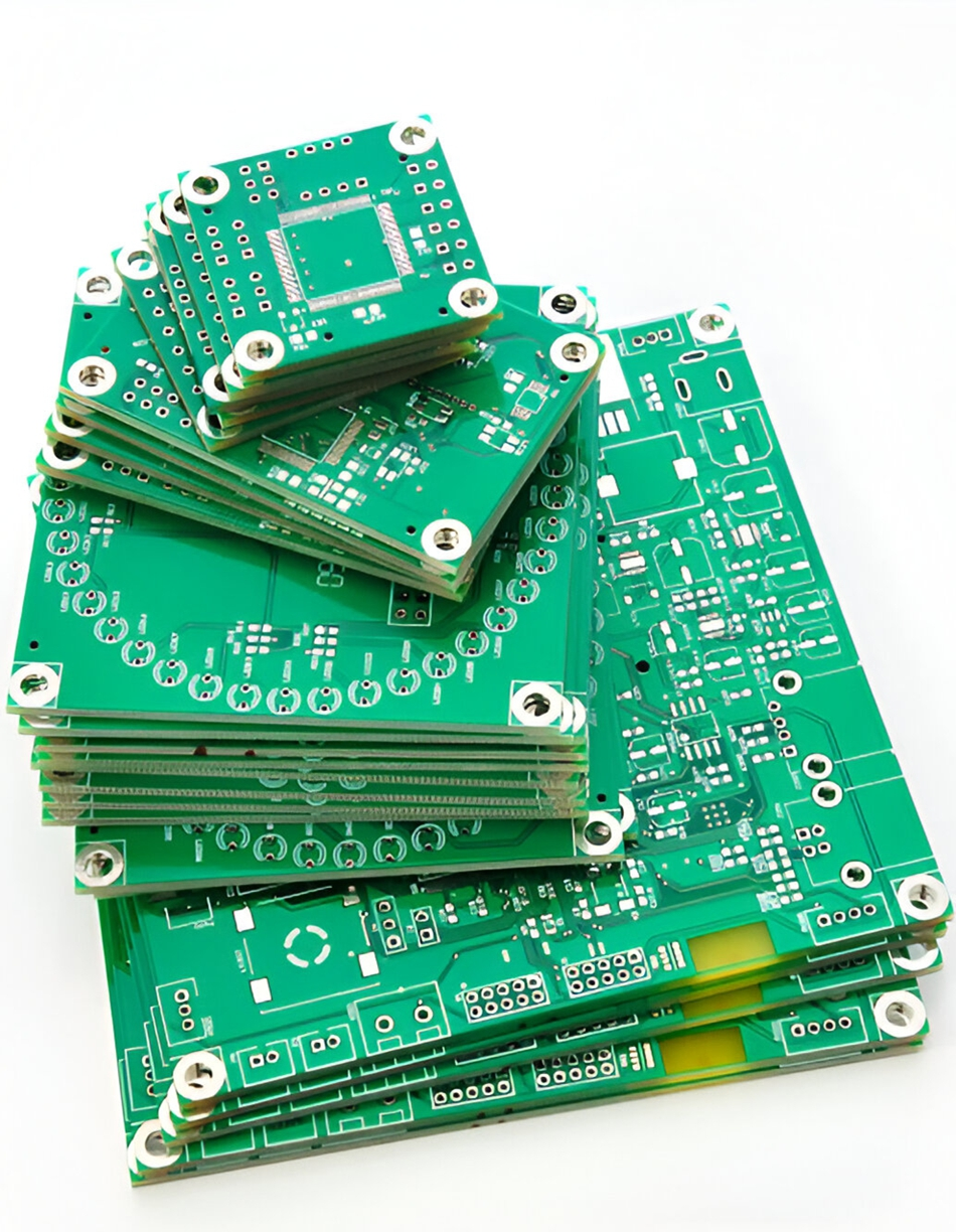
How AIVON Supports Your PCB Solder Mask Requirements
At AIVON, we recognize that each printed circuit board project comes with its own specific demands. Whether your design calls for the extreme precision and uniform thickness of a Dry Film Solder Mask or the cost-effective and swift application of a Liquid Photoimageable (LPI) Solder Mask, our dedicated team is prepared to deliver high-quality manufacturing solutions. We provide both solder mask technologies, along with extensive customization options, to ensure that your boards achieve optimal performance and unwavering reliability, perfectly aligning with your design specifications.
Our advanced manufacturing facilities, coupled with the expertise of our seasoned engineers, enable us to guide you through the intricate selection process. We offer tailored insights and recommendations specific to your application, ensuring you make the most informed decision. From initial prototyping to large-scale PCB mass production, AIVON is committed to fabricating PCBs that not only meet but exceed your exact needs, delivered punctually and within your budgetary constraints.
Conclusion: Making an Informed Solder Mask Choice for Your PCB
The decision between Dry Film Solder Mask and Liquid Photoimageable (LPI) Solder Mask for your PCB project hinges on a careful evaluation of performance demands, cost implications, and manufacturing timelines. Dry Film distinguishes itself through its exceptional precision and consistent thickness, making it the ideal selection for high-density, high-frequency, and mission-critical applications, albeit with a higher cost and longer processing duration. Conversely, LPI offers a more budget-friendly and faster application process, making it an excellent choice for standard designs, prototyping, and large-volume consumer electronics, though it may not offer the same level of thickness uniformity or ultra-fine precision.
By thoroughly understanding the advantages and cost comparisons of each — Dry Film's superior durability and exacting precision versus LPI's economic efficiency and rapid application — you can confidently select the solder mask solution that best supports your project’s objectives. At AIVON, we are here to assist you in navigating these crucial decisions, ensuring we deliver outstanding PCB solutions meticulously tailored to your specifications. Whether your priority is uncompromised precision or cost-effective manufacturing, our expertise is at your disposal to bring your design concepts to fruition.