Introduction
In the rapidly evolving field of electronics, printed circuit board (PCB) reliability remains a critical concern for engineers and designers. As devices become smaller and more complex, ensuring robust solder joint reliability and minimizing via failure modes are paramount. Via-in-pad technology has emerged as a powerful solution to address these challenges, offering improved space efficiency and electrical performance. This article explores how via-in-pad design enhances PCB reliability, tackles common via failure modes, and contributes to improving PCB lifespan. Written from the perspective of a PCB design expert, the content provides logical and structured insights for electrical engineers seeking to optimize their designs for durability and performance while adhering to industry standards.
What Is Via-in-Pad Technology and Why It Matters
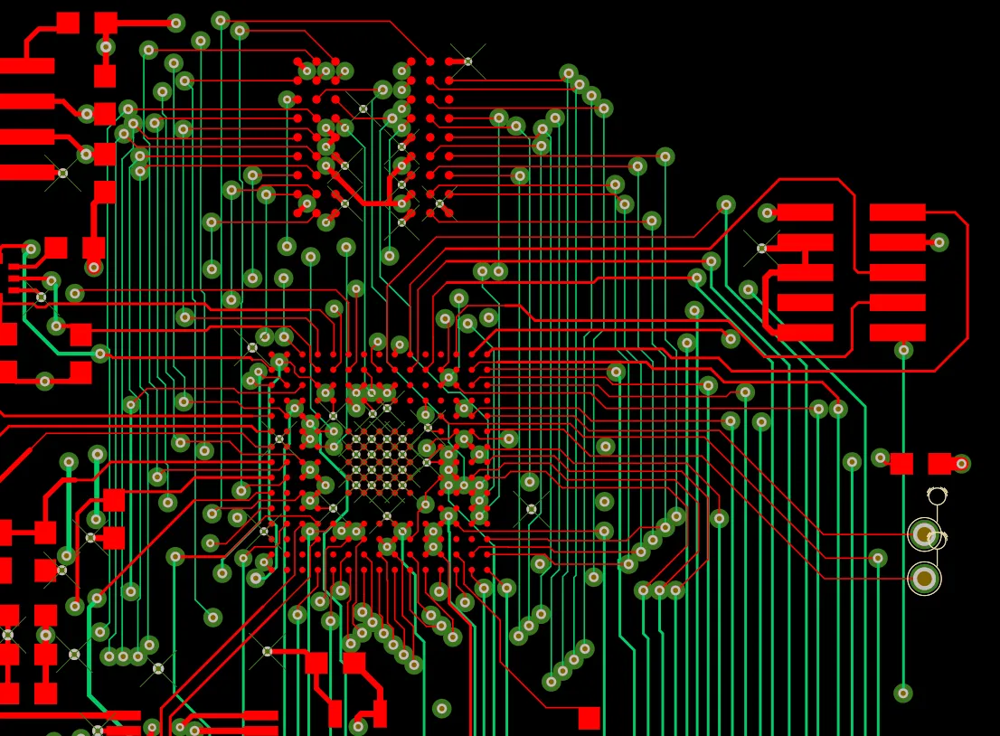
Via-in-pad technology refers to a PCB design technique where vias are placed directly within the component pads, rather than adjacent to them. This approach is particularly valuable in high-density interconnect (HDI) designs, where space constraints demand innovative routing solutions. By integrating vias into the pads, designers can reduce the board's footprint, shorten signal paths, and improve thermal management. This is especially critical for fine-pitch components like ball grid arrays (BGAs) and quad flat no-leads (QFNs), which require precise connections.
Related Reading: Stacked Via vs. Via in Pad: Which Via Technology is Best for BGA Routing?
The significance of via-in-pad technology lies in its impact on PCB reliability. Traditional via placements can lead to longer traces, increasing signal loss and electromagnetic interference. In contrast, via-in-pad designs minimize these issues, enhancing signal integrity. Additionally, this technique supports better solder joint reliability by optimizing the connection between components and the board, a key factor in extending PCB lifespan.
Technical Principles of Via-in-Pad Technology
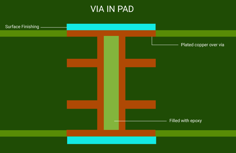
Understanding the engineering behind via-in-pad technology is essential for leveraging its benefits. In this design, the via is typically filled with a conductive or non-conductive material to create a flat surface for soldering. This process, often referred to as via-in-pad plated over (VIPPO) or plugged and overfilled vias (POFV), ensures that the via does not interfere with the component attachment during assembly.
One primary advantage is the reduction of parasitic inductance and capacitance due to shorter interconnects. For high-frequency applications, this translates to improved signal performance. Moreover, placing vias directly under components aids in heat dissipation, as the via can act as a thermal conduit to inner layers or a heat sink. However, challenges exist, such as potential voiding during soldering if the via is not properly filled, which can compromise solder joint reliability.
Via failure modes are a significant concern in PCB design. Common issues include barrel cracking due to thermal expansion mismatches and via delamination caused by mechanical stress. Via-in-pad technology can mitigate some of these risks by reducing stress concentration points, but careful design and manufacturing processes are necessary to avoid defects.
Related Reading: Troubleshooting Common Via-in-Pad Issues in PCB Design
Impact on Solder Joint Reliability
Solder joint reliability is a cornerstone of PCB performance, especially in environments with thermal cycling or mechanical vibration. Via-in-pad technology directly influences this reliability by altering how solder interacts with the pad and component. When vias are placed within pads, the solder must form a uniform joint over a potentially uneven surface if the via is not filled correctly. Industry standards, such as IPC-A-600K, emphasize the importance of via filling and surface planarity to prevent defects like voids or insufficient solder coverage.
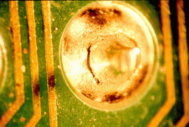
Improperly managed via-in-pad designs can lead to solder wicking, where molten solder flows into the via, leaving insufficient material for the joint. This weakens the connection and increases the risk of failure under stress. To counter this, filled vias are recommended, ensuring a stable platform for soldering. This approach enhances the mechanical strength of the joint, directly contributing to improving PCB lifespan.
Thermal cycling tests, guided by standards like JEDEC J-STD-020E, often reveal the durability of solder joints. Designs incorporating via-in-pad technology, when executed with proper filling and plating, show improved resistance to fatigue cracking compared to traditional layouts. This is particularly beneficial for applications in automotive and aerospace sectors, where reliability under extreme conditions is non-negotiable.
Via Failure Modes and Mitigation Strategies
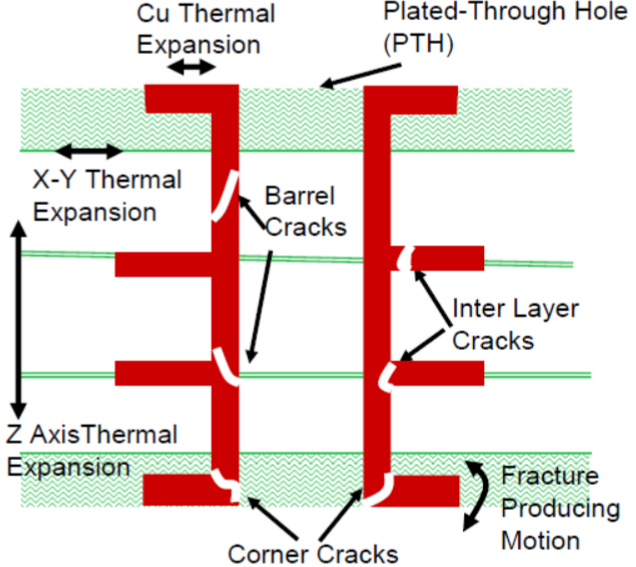
Via failure modes can significantly undermine PCB reliability if not addressed during the design phase. Common failure mechanisms include via barrel cracking, where the copper plating inside the via fractures due to thermal expansion differences between materials. Another issue is via-to-pad separation, often caused by mechanical stress or poor adhesion during manufacturing.
Via-in-pad technology introduces unique considerations for failure mitigation. Since the via is located directly under the component, any defect in the via structure can directly impact the solder joint. For instance, incomplete via filling can trap air or flux, leading to outgassing during reflow soldering and creating voids. Standards like IPC-6012E provide guidelines for via filling and inspection to ensure structural integrity.
To minimize these risks, designers must specify appropriate via filling materials and processes. Conductive epoxy or copper-filled vias offer robust solutions for maintaining electrical and thermal conductivity. Additionally, controlling the aspect ratio of the via, as recommended by IPC standards, prevents issues during plating and filling. By addressing these factors, via-in-pad designs can significantly reduce failure rates and enhance overall PCB reliability.
Practical Solutions for Implementing Via-in-Pad Technology
Adopting via-in-pad technology requires careful planning to ensure its benefits are realized without introducing new risks. Below are actionable best practices for electrical engineers looking to integrate this approach into their designs.
- Specify via filling: Always opt for filled vias to create a flat soldering surface. Non-conductive epoxy or conductive materials can be used based on thermal and electrical requirements. This aligns with IPC-A-600K guidelines for surface finish and planarity.
- Optimize pad design: Ensure pad dimensions accommodate the via size and filling process. Oversized pads can compensate for minor misalignments during assembly, improving solder joint reliability.
- Control manufacturing parameters: Work closely with fabrication teams to maintain tight tolerances during via drilling and filling. Standards like IPC-6012E provide acceptance criteria for via quality.
- Perform reliability testing: Conduct thermal cycling and vibration testing per JEDEC J-STD-020E to validate the design under real-world conditions. This helps identify potential via failure modes early.
By following these practices, engineers can maximize the advantages of via-in-pad technology while minimizing risks to PCB reliability. Proper implementation directly contributes to improving PCB lifespan, especially in high-density applications.
Design Considerations for Long-Term Reliability
Beyond immediate implementation, long-term PCB reliability hinges on strategic design choices. Via-in-pad technology must be paired with material selections and layout strategies that withstand environmental stresses. For instance, choosing a substrate with a low coefficient of thermal expansion (CTE) reduces stress on vias during temperature changes. This is particularly relevant for multilayer boards where inner layer connections are critical.
Layer stackup design also plays a role. Positioning vias in pads on outer layers simplifies manufacturing but requires robust filling to prevent solder issues. Conversely, buried or blind vias in HDI designs, while complex, can benefit from via-in-pad techniques to save space and improve signal integrity. Adhering to IPC-6012E ensures that these configurations meet performance and quality standards.
Finally, simulation tools can predict stress points and thermal behavior before fabrication. Finite element analysis (FEA) helps identify potential via failure modes under various conditions, allowing for design adjustments. This proactive approach ensures that via-in-pad technology contributes positively to PCB reliability over the product's lifecycle.
Conclusion
Via-in-pad technology offers a compelling solution for enhancing PCB reliability in modern electronics design. By integrating vias directly into component pads, this approach improves space efficiency, signal integrity, and thermal management. However, its success depends on meticulous design and manufacturing practices to ensure solder joint reliability and mitigate via failure modes. Adherence to industry standards like IPC-6012E and JEDEC J-STD-020E provides a framework for achieving consistent results. For electrical engineers, adopting via-in-pad technology represents a strategic step toward improving PCB lifespan and meeting the demands of high-density, high-performance applications.
FAQs
Q1: How does via-in-pad technology improve PCB reliability?
A1: Via-in-pad technology enhances PCB reliability by reducing signal path lengths and improving thermal dissipation. This minimizes signal loss and stress on components, leading to stronger solder joints. When vias are properly filled per IPC-A-600K standards, risks of voids or wicking are reduced, ensuring long-term durability in demanding environments.
Q2: What are common via failure modes in via-in-pad designs?
A2: Common via failure modes include barrel cracking from thermal expansion and via-to-pad separation due to mechanical stress. Incomplete filling can also cause outgassing during soldering, leading to voids. Following IPC-6012E guidelines for via construction helps mitigate these issues and maintain structural integrity.
Q3: How can engineers ensure solder joint reliability with via-in-pad technology?
A3: Engineers can ensure solder joint reliability by specifying filled vias and optimizing pad designs. Conductive or non-conductive filling prevents solder wicking, while adherence to IPC-A-600K ensures surface planarity. Testing under JEDEC J-STD-020E conditions also validates joint strength under thermal stress.
Q4: What role does via-in-pad technology play in improving PCB lifespan?
A4: Via-in-pad technology contributes to improving PCB lifespan by enhancing connection stability and reducing stress points. Properly implemented designs resist thermal and mechanical fatigue, key factors in long-term failures. Compliance with industry standards ensures consistent performance, extending the operational life of the board.
References
IPC-6012E - Qualification and Performance Specification for Rigid Printed Boards. IPC, 2020.
IPC-A-600K - Acceptability of Printed Boards. IPC, 2020.
JEDEC J-STD-020E - Moisture/Reflow Sensitivity Classification. JEDEC, 2014.