What Are Plated Through-Holes and Why Are They Key for High-Current PCBs?
Plated through-holes (PTHs) are fundamental features in printed circuit board (PCB) construction, serving as vital conduits for electrical connections between different layers and as mounting points for through-hole components. Unlike non-plated holes, PTHs are coated with a conductive material, typically copper, which provides both electrical conductivity and enhanced mechanical stability. Their capacity to conduct current without degradation or excessive heat buildup directly influences a PCB's overall performance and safety, especially in demanding applications.
In the realm of high-current PCB design, PTHs frequently function as critical pathways for substantial power delivery. If not designed correctly, these holes can become bottlenecks, leading to localized heat accumulation, significant voltage drops, or even catastrophic board failure. Therefore, mastering the techniques to maximize their current-carrying capability is paramount for developing robust and efficient electronic designs.
What Factors Determine a PTH's Current Rating?
The current rating of a plated through-hole—the maximum current it can safely conduct—is influenced by several interconnected design parameters. Understanding each factor is crucial for optimizing current capacity and ensuring long-term reliability.
Copper Plating Thickness
The thickness of the copper layer within the through-hole is a primary determinant of its current-carrying capability. A thicker copper plating reduces electrical resistance, allowing a greater flow of current without generating excessive heat. While standard PCBs might feature PTH copper plating thickness between 0.8 to 1.2 mils (20 to 30 micrometers), high-current applications often benefit from increasing this to 2 mils (50 micrometers) or more. Heavy copper PCB not only boosts current capacity but also improves durability during thermal cycling by better resisting expansion and contraction from temperature changes. However, designers must balance increased manufacturing costs with performance requirements.
Hole Diameter and Aspect Ratio
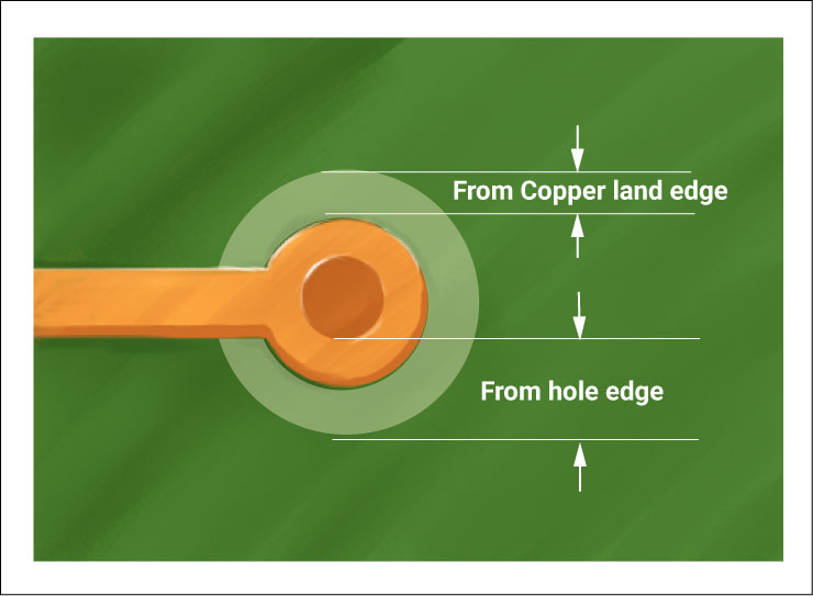
The diameter of the PTH directly impacts its current capacity; larger holes offer increased surface area for copper plating, which translates to lower resistance and improved current flow. For high-current designs, opting for larger PTH diameters, typically 0.040 to 0.060 inches (1 to 1.5 mm), is advisable, provided they fit within layout constraints. The aspect ratio (the ratio of board thickness to hole diameter) also plays a critical role. A lower aspect ratio (e.g., a thinner board or larger hole) facilitates more uniform copper plating, which is vital for consistent current capacity, whereas a high aspect ratio can lead to uneven plating and create vulnerable points.
Thermal Management in PTH Design
Effective heat dissipation is a critical consideration when high currents are involved. PTHs can become significant hot spots if the heat generated by current flow is not managed efficiently. Suboptimal thermal management can result in issues such as delamination, cracking, or even complete failure of the PCB. Later sections will detail specific strategies to mitigate thermal challenges and ensure reliable operation under high-current conditions.
How Can You Increase PTH Current Capacity in Designs?
Once the factors influencing PTH current rating are understood, designers can implement specific techniques to enhance current capacity in their PCB layouts. These methods are designed to push the limits of high-current applications while maintaining circuit reliability.
Optimizing Copper Plating and Multiple PTHs
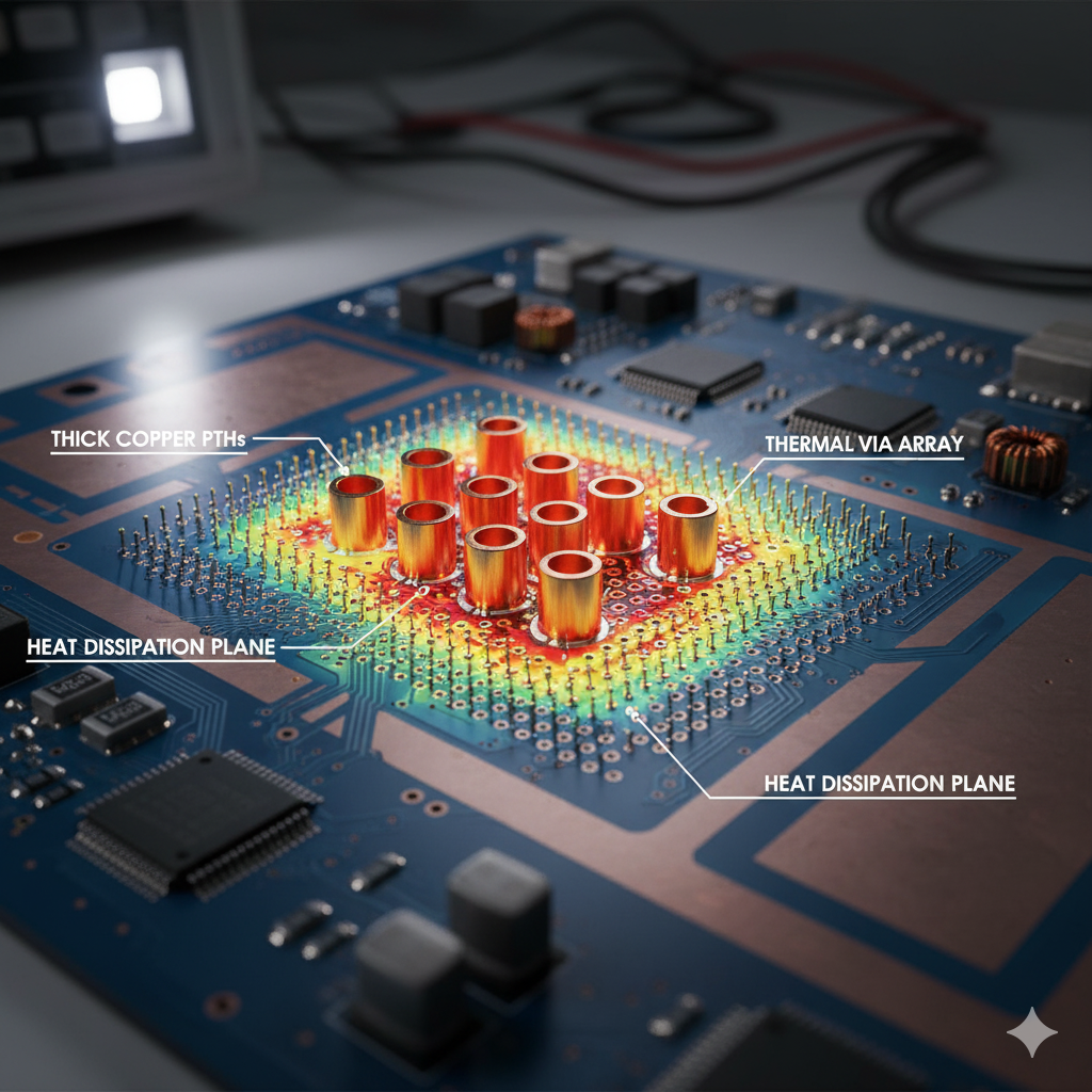
To start, increasing the copper plating thickness inside the PTH significantly reduces resistance and enhances current capacity. When specifying PCB designs, request heavier copper plating for PTHs, especially in critical power delivery zones. For example, moving from a standard 1 oz/ft² (35 micrometers) to 2 oz/ft² (70 micrometers) or higher copper weight can yield substantial improvements. This principle also extends to connected traces; the entire current path must be optimized. It's also crucial to ensure uniform plating within the holes, as inconsistencies can create high-resistance points and potential failure sites. Collaborating with your PCB manufacturer on quality control for plating consistency is essential. For extremely high-current applications, a single PTH might not suffice. A practical solution involves using multiple PTHs in parallel for the same connection, which distributes the current load, reduces stress on individual holes, and minimizes heat buildup. This approach also adds redundancy.
Implementing Thermal Management Techniques
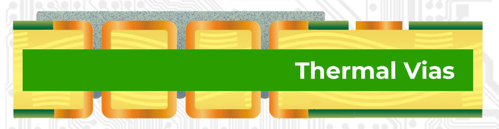
Thermal vias are small, plated holes strategically placed near high-current PTHs to facilitate heat dissipation. Although they do not carry significant current themselves, they provide pathways for heat to transfer from hot spots to larger copper areas or ground planes, or even to a heat sink. For effective thermal management in PTH design, array thermal vias (typically 0.010 to 0.012 inches or 0.25 to 0.3 mm in diameter) around power component mounting holes or high-current PTHs. A grid pattern can maximize their effect, but care must be taken not to compromise the board's structural integrity by overcrowding the area.
Selecting Appropriate Materials
The choice of PCB base material significantly influences its ability to handle high currents and manage heat. While standard FR4 PCB is suitable for many applications, high-current designs may benefit from high-temperature laminates or materials with superior thermal conductivity. These materials can withstand the elevated temperatures associated with high-current PTHs and prevent long-term degradation. Additionally, ensuring that solder used for through-hole components has a high melting point and good thermal stability is crucial, as poor solder joints can introduce high-resistance points that undermine an otherwise optimized PTH design.
What Are Best Practices for High-Current PCB Design with PTH?
Beyond specific techniques, integrating best practices throughout the PCB design process is vital for optimizing performance in high-current applications. These guidelines focus on creating reliable and efficient boards.
Complement PTH Capacity with Wide Traces
Even with optimized PTHs, the traces connected to them must also be capable of handling the current load. Employing wider traces reduces resistance and prevents bottlenecks in the current path. As a general guideline, for every 10 amps of current, a trace width of at least 0.1 inches (2.54 mm) is recommended for 1 oz/ft² copper at room temperature, adjustable based on copper weight and operating conditions. Utilizing online calculators or design software can help determine the precise trace width required, ensuring that no part of the circuit becomes a weak link.
Minimize Aspect Ratio and Perform Thermal Simulations
As discussed, a high aspect ratio can lead to uneven copper plating and reduced current capacity. Design PCBs with thinner boards or larger hole diameters where feasible to maintain a low aspect ratio, ideally 6:1 or less, to ensure uniform plating and reliable performance in high-current PTHs. Before finalizing a design, conduct thermal simulations to model the PCB's behavior under high-current conditions. These tools can predict temperature rises around PTHs and pinpoint potential hotspots. Addressing thermal issues during the design phase can avert high PCB cost or field failures; aim for a maximum temperature rise of 10-20°C above ambient in critical areas for long-term reliability.