Introduction
Fine-pitch components present unique challenges in PCB assembly, particularly when it comes to ensuring reliable solder joints without defects like bridging or insufficient wetting. As electronic devices shrink and component densities increase, engineers must prioritize pad-to-pad spacing to accommodate precise fine pitch components soldering processes. Proper spacing prevents solder bridges that can lead to shorts, while also supporting robust mechanical and electrical connections. This article explores the principles behind optimal pad spacing, pad types, and footprint design strategies tailored for high-reliability assemblies. By focusing on industry best practices, designers can troubleshoot common issues and achieve consistent results in production. Understanding these elements is crucial for electric engineers working on compact, high-performance boards.
Understanding Fine-Pitch Components and Pad-to-Pad Spacing
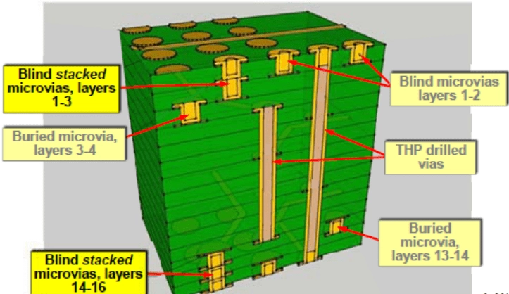
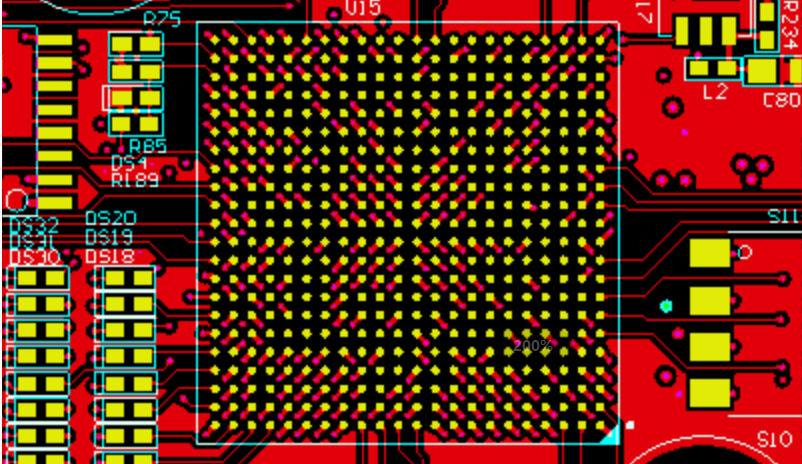
Fine-pitch components, such as BGAs, QFNs, and CSPs with closely spaced leads or balls, demand meticulous attention to pad-to-pad spacing on the PCB. Pad spacing fine pitch refers to the minimum distance between adjacent copper pads, which must account for solder paste deposition, reflow dynamics, and manufacturing tolerances. Too narrow spacing risks solder bridging during reflow, while excessive spacing can weaken joint standoff or complicate routing. This spacing directly influences the success of fine pitch components soldering, where even minor variations in paste volume or component placement can cause failures. Engineers evaluate spacing based on component pitch, pad geometry, and assembly process capabilities to ensure manufacturability. Balancing these factors aligns with standards like IPC-7351, which guides land pattern development for surface mount devices.
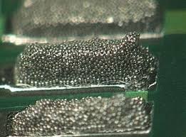
In practice, pad-to-pad spacing serves as a buffer zone that isolates individual solder joints, promoting uniform heating and minimizing interactions between neighboring fillets. For instance, in dense arrays, insufficient spacing amplifies risks from solder paste slumping or wicking during printing. Troubleshooting starts with verifying design files against component datasheets and process windows. Why it matters becomes evident in high-volume production, where bridging defects can exceed 5% yield loss if unaddressed. Optimal spacing enhances long-term reliability by reducing stress concentrations in joints exposed to thermal cycling.
Technical Principles of Pad Design for Fine-Pitch Reliability
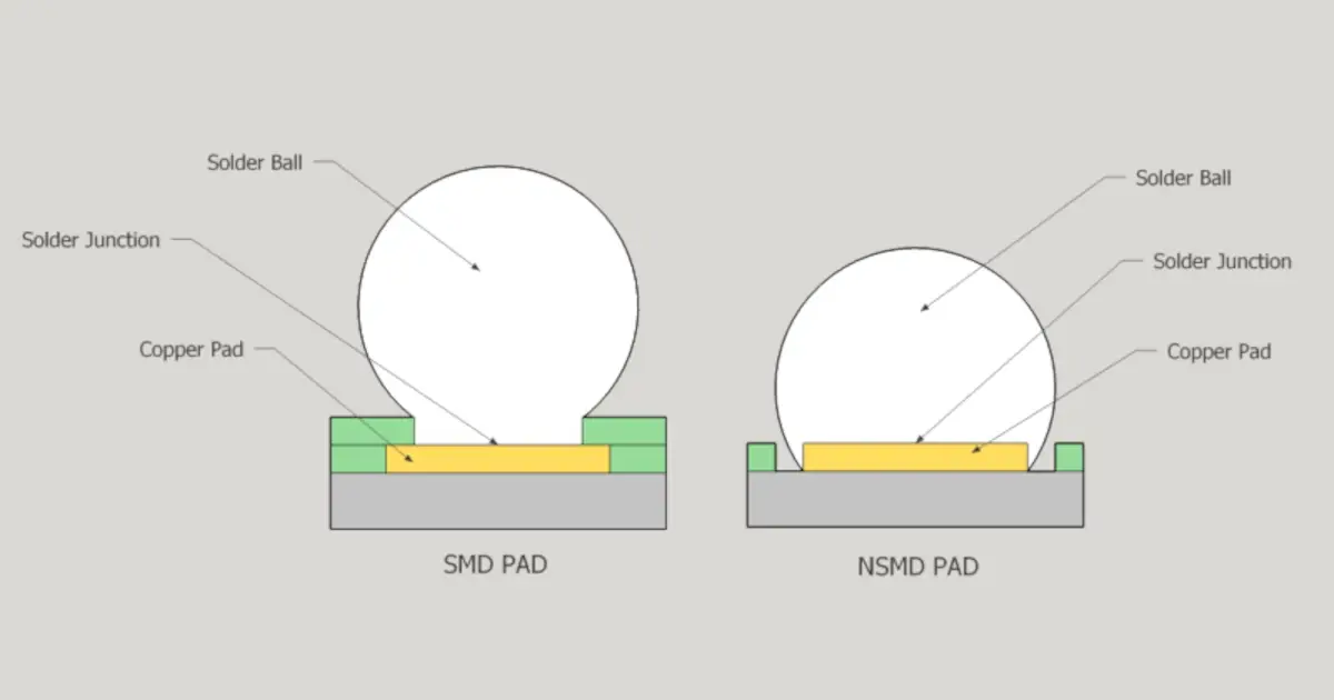
Pad design forms the foundation of reliable connections, with solder mask defined pads (SMD) and non-solder mask defined pads (NSMD) offering distinct behaviors in fine-pitch applications. SMD pads feature a solder mask opening smaller than the exposed copper, which confines the solder joint and reduces bridging risks by controlling paste spread. NSMD pads, conversely, have a mask opening larger than the copper pad, allowing the joint to form freely around the pad edges for greater volume and compliance. The nsmd pads advantages shine in fine pitch components soldering, as they provide superior shear strength and accommodate CTE mismatches between the component and board. IPC-7351 outlines land pattern criteria, including density levels that adjust pad size and spacing for most, nominal, or least dense configurations to suit assembly needs.
Pad-to-pad spacing integrates with these pad types through solder mask clearance, typically set to prevent mask encroachment that could alter joint formation. In IC package footprint design, engineers calculate spacing as a function of lead pitch minus fabrication tolerances, ensuring room for trace escape routing without violating minimum rules. Solder mask expansion around pads maintains electrical isolation while allowing reflow fillet formation. For fine-pitch arrays, NSMD structures excel by enabling smaller effective pad areas, which frees space between pads and eases high-density routing. This approach minimizes tombstoning or floating components during reflow, common pitfalls in tight layouts.
Reflow dynamics further underscore spacing importance, as molten solder seeks to bridge gaps under surface tension if pad-to-pad distances fall below process control limits. Standards like J-STD-001 specify criteria for acceptable joint appearance and hole fill, indirectly guiding spacing to avoid voids or excesses. Thermal management plays a role too, with closer spacing potentially leading to uneven heating in dense areas, exacerbating defects. Engineers model these interactions using simulation tools to predict joint profiles before prototyping. Ultimately, principled design rooted in these mechanisms yields assemblies that withstand vibration, humidity, and cycling without premature failure.
Best Practices for Optimal Pad-to-Pad Spacing in IC Package Footprint Design
Start IC package footprint design by selecting pad type based on pitch and reliability priorities, favoring NSMD for pitches where joint compliance outweighs bridging concerns. Reference IPC-7351 density levels to scale pad dimensions and derive pad spacing fine pitch values that match your fabricator's capabilities. Maintain solder mask clearance at least equal to the minimum trace-to-pad rule, typically expanding 0.1 mm beyond pad edges to avoid webbing. For fine pitch components soldering, collaborate with stencil designers to match aperture reductions, often 10-20% smaller than pads, which complements tight spacing by controlling paste volume.
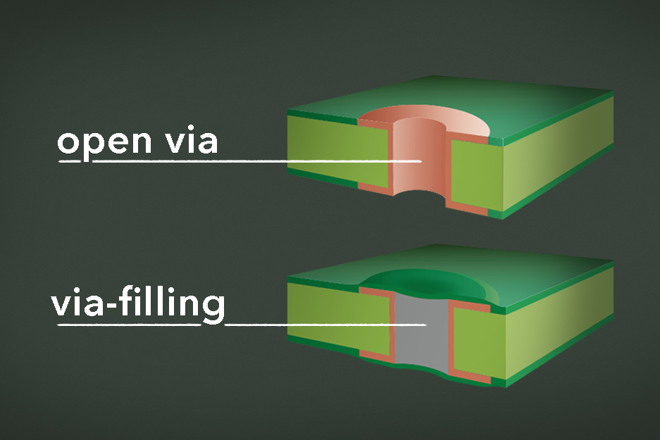
Incorporate via-in-pad strategies judiciously, ensuring filled or tented vias do not encroach on adjacent pad areas and disrupt spacing. Route traces under pads only if dog-bone escapes fit within the array without compressing inter-pad gaps. Validate designs through DFM checks, simulating paste printing and reflow to flag potential bridges. Practical troubleshooting involves inspecting paste deposits under microscope for uniformity across fine-pitch rows. Adjust stencil thickness downward for ultra-fine pitches to enhance release and minimize bridging propensity.
Profile reflow ovens to achieve linear ramp rates, preventing rapid melting that pulls solder across narrow spaces. Post-reflow, X-ray or AOI verifies joint integrity, focusing on bridge-free fillets with proper heel-toe wetting. For rework, wider spacing aids site dressing without damaging neighbors. These practices, grounded in process data, consistently deliver yields above 99% for fine-pitch assemblies. Regularly audit supplier DFM reports to refine spacing rules iteratively.
Troubleshooting Common Issues in Fine-Pitch Pad Spacing
Bridging tops the list of defects in pad spacing fine pitch scenarios, often stemming from excessive paste volume or mask misalignment. Inspect stencils for aperture bridging or damage, and recalibrate printers for snap-off distances that avoid smearing. If bridges persist post-reflow, extend pad-to-pad spacing incrementally while preserving footprint integrity per IPC-7351 guidelines. Insufficient wetting, marked by de-wetted pads, signals poor fluxing or oxidation; preheat boards adequately to activate flux before peak temperatures.
Tombstoning in QFN or CSP arrays arises from uneven heating across tight spacing, resolved by adding thermal reliefs or adjusting conveyor speeds. For NSMD pads, monitor mask undercut that enlarges effective openings, potentially worsening bridging; specify tighter mask registration in fab notes. Solder beading under components points to outgassing or contamination, mitigated by plasma cleaning before assembly. Systematic root-cause analysis, using 3D SPI and cross-sectioning, pinpoints spacing-related failures efficiently.
Yield mapping reveals patterns, like edge bridging from warped boards, prompting carrier fixturing. Document fixes in ECAD libraries for reuse, ensuring team-wide consistency. These troubleshooting steps transform chronic issues into reliable processes.
Conclusion
Achieving optimal pad-to-pad spacing demands a holistic approach integrating pad types, footprint design, and process controls for fine-pitch success. NSMD pads advantages in joint reliability, paired with precise solder mask defined pads where bridging looms large, guide engineers toward robust assemblies. Adhering to IPC-7351 and J-STD-001 ensures compliance and manufacturability. Practical implementation, from stencil optimization to reflow profiling, minimizes defects and boosts yields. Electric engineers benefit from proactive DFM and troubleshooting to deliver high-density boards that perform reliably in the field. Mastering these elements elevates design quality across projects.
FAQs
Q1: What are the key nsmd pads advantages in fine pitch components soldering?
A1: NSMD pads offer superior solder joint strength and compliance due to larger mask openings that allow full encapsulation of the copper pad. They facilitate better stress relief during thermal cycling and enable tighter routing in dense IC package footprint design. While SMD pads control bridging better in some ultra-fine cases, NSMD excels for reliability in pitches above critical thresholds. Always verify against IPC-7351 for your density level.
Q2: How does pad spacing fine pitch impact solder bridging during reflow?
A2: Narrow pad spacing fine pitch heightens bridging risks as surface tension draws molten solder between pads if paste volume exceeds joint needs. Optimal spacing, derived from component pitch and tolerances, provides isolation for uniform fillet formation. Stencil apertures tuned to 80-90% of pad area complement this by limiting transfer. Troubleshoot with SPI to adjust printer parameters proactively.
Q3: When should solder mask defined pads be used over NSMD in IC package footprint design?
A3: Opt for solder mask defined pads in ultra-fine pitches or high-vibration environments where confinement prevents bridging and enhances adhesion. They suit applications needing precise joint standoff, though at the cost of reduced compliance compared to NSMD. Balance with J-STD-001 criteria for joint criteria. Test prototypes to confirm assembly yields before commitment.
Q4: What role does IPC-7351 play in fine pitch components soldering layouts?
A4: IPC-7351 standardizes land patterns with scalable density levels, dictating pad size, shape, and spacing for reliable fine pitch components soldering. It accounts for fabrication variances to ensure paste printing and reflow success. Use it to generate footprints that align with supplier capabilities, minimizing defects like bridging or opens.
References
IPC-7351C — Generic Requirements for Surface Mount Design and Land Pattern Standard. IPC, 2014
J-STD-001H — Requirements for Soldered Electrical and Electronic Assemblies. IPC, 2020
IPC-2221B — Generic Standard on Printed Board Design. IPC, 2012