Introduction
Glass-reinforced printed circuit boards form the backbone of reliable electronics in demanding applications, where mechanical strength and electrical performance converge. PCB stackup design defines the precise arrangement of conductive layers, insulating cores, and prepregs, all reinforced with glass fibers to enhance dimensional stability and resist thermal stresses. In high-speed designs, optimizing this layer stackup design becomes essential for maintaining signal integrity and ensuring an effective power distribution network. Poor stackup choices lead to issues like crosstalk, impedance mismatches, and voltage droop, compromising overall system reliability. Engineers must balance factors such as dielectric properties, layer symmetry, and plane proximity to achieve optimal performance. This article explores PCB design guidelines tailored to glass-reinforced materials, providing structured insights for electric engineers focused on multilayer boards.
What Is Glass-Reinforced PCB Stackup and Why It Matters
Glass-reinforced PCB stackup refers to the vertical buildup of a board using materials where woven glass fabric is impregnated with epoxy resin, creating rigid cores and prepregs that separate copper foils. These glass-epoxy composites, common in standard rigid PCBs, provide high tensile strength and low coefficient of thermal expansion compared to unreinforced alternatives. The stackup specifies thicknesses, material types, and sequencing from top signal layer to bottom, influencing electrical, thermal, and mechanical behaviors. Signal integrity depends on consistent impedance and minimal reflections, while the power distribution network relies on low-inductance paths for stable voltage delivery.
This design matters profoundly in modern electronics, where rising clock speeds amplify sensitivity to stackup variations. Asymmetric arrangements cause warpage during fabrication or reflow, leading to assembly defects. Effective layer stackup design mitigates electromagnetic interference, supports high-frequency signals, and ensures uniform power delivery across components. For electric engineers, adhering to PCB stackup principles directly impacts yield rates and long-term reliability in compact, high-density layouts.
Technical Principles Behind Glass-Reinforced Stackups
The core principle of glass-reinforced stackups lies in the dielectric interface between copper layers, where glass fabric orientation and resin content determine permittivity and loss tangent. These properties control characteristic impedance for traces routed as microstrip or stripline configurations. In multilayer boards, cores offer structural integrity, while thinner prepregs fine-tune separations for impedance matching. Signal propagation speed and attenuation hinge on dielectric thickness uniformity, as variations introduce phase shifts and losses.
Return current paths form another foundational mechanism, with adjacent reference planes providing low-impedance loops essential for signal integrity. Ground planes shield signals from crosstalk, confining fields between planes rather than radiating outward. For power distribution networks, closely spaced power and ground planes create distributed capacitance, decoupling high-frequency noise without excessive discrete components. Thermal expansion mismatch between glass fibers and copper necessitates symmetric constructions to equalize stresses across the stackup.
IPC-2221B outlines key multilayer design requirements, emphasizing balanced material distribution to prevent bow and twist. Resonance in PDN occurs when plane inductance interacts with bypass capacitors, underscoring the need for broad via stitching to lower effective impedance.
Optimizing Layer Arrangement for Signal Integrity
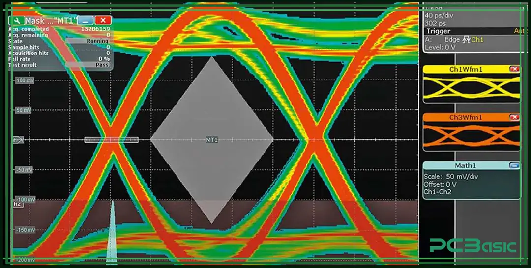
Engineers prioritize placing high-speed signal layers between full ground planes to create stripline routing, which offers superior shielding over microstrip. This arrangement confines electromagnetic fields, reducing crosstalk by up to significant margins through field containment. Reference plane integrity demands continuous copper pours, avoiding splits under traces to prevent return path detours that increase loop inductance. Differential pairs benefit from tight coupling within the same layer, flanked by ground for common-mode rejection.
Impedance control requires precise dielectric thicknesses, with glass-reinforced prepregs selected for consistent stack height. Vias transitioning layers introduce stubs that reflect signals if not back-drilled, so blind or buried vias minimize discontinuities. Length matching for clock lines and data buses preserves timing margins in synchronous systems.
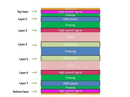
In eight-layer stackups, alternating signal-ground-signal patterns from outer to inner layers optimizes density while preserving integrity. Core selection influences overall rigidity, with thicker glass-reinforced cores supporting finer inner layer features without flexing during lamination.
Enhancing Power Distribution Network Through Stackup Choices
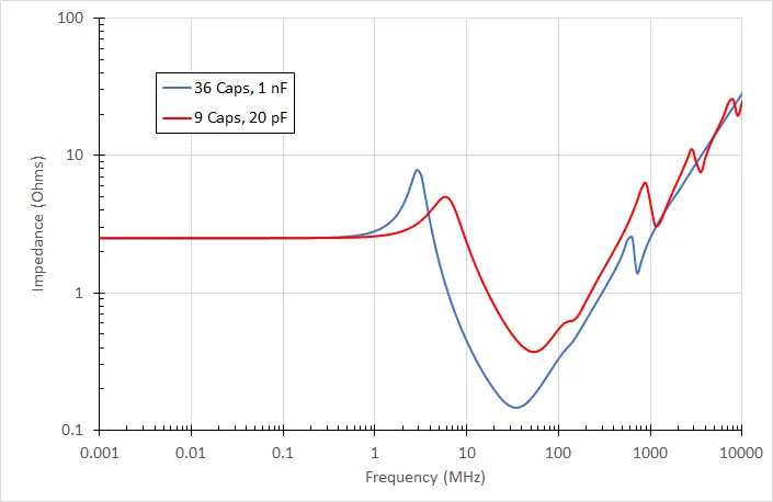
Power distribution networks thrive on minimal inductance between supply and return planes, achieved by dedicating inner layers to solid power and ground pours. Placing these planes adjacent, such as layer 3 power over layer 4 ground, forms a low-inductance capacitor with values scaling inversely with separation. This distributed capacitance filters ripple currents from switching regulators, stabilizing voltage rails across the board.
Via stitching connects segmented plane areas, providing current sharing and reducing slot antenna effects that radiate EMI. Power islands for multiple voltages require careful partitioning, with moats and stitching to isolate domains without gaps under signals. Glass-reinforced materials maintain plane flatness under thermal cycling, preventing microcracks that degrade PDN performance.
Decoupling capacitors mount directly on power-ground transitions, leveraging the stackup's proximity for sub-nanohenry paths. Engineers simulate PDN impedance targets below milliohms up to GHz frequencies, guiding layer assignments.
Best Practices in PCB Stackup Design Guidelines
Follow symmetric layer stackup design by mirroring materials above and below the neutral axis, countering warpage from CTE differences in glass-epoxy and copper. For a six-layer board, pair thin prepregs symmetrically around thick cores, ensuring equal buildup on both sides. IPC-6012E specifies performance criteria for rigid boards, including bow and twist limits that symmetric stackups help achieve.
Select glass-reinforced prepregs with matching resin content across layers to avoid lamination voids. Route critical signals on inner layers for better integrity, reserving outer layers for low-speed or connectors. Incorporate at least one ground plane per two signal layers, enhancing shielding and PDN decoupling.
Test stackup viability through field solver tools for impedance and loss profiles before fabrication. Collaborate early with fabricators on drill aspect ratios feasible with glass-reinforced thicknesses.
Troubleshooting Common Stackup Challenges
Warpage emerges as a primary issue in asymmetric glass-reinforced stackups, exacerbated by reflow temperatures causing resin softening. Measure bow and twist per industry methods, targeting values under allowable thresholds for component placement. Remedies include redesigning for balance or using higher glass transition materials judiciously.
PDN resonance peaks manifest as voltage overshoot, traced to insufficient plane capacitance or poor via density. Analyze target impedance curves to identify and mitigate peaks with added stitching. Crosstalk spikes in simulations signal inadequate plane referencing, resolved by layer resequencing.
Signal reflections from impedance steps demand uniform trace geometries across layer transitions.
Conclusion
Mastering glass-reinforced PCB stackup design hinges on strategic layer arrangement that safeguards signal integrity and bolsters power distribution networks. Symmetric constructions, adjacent plane pairs, and reference shielding form the pillars of robust PCB design guidelines. Electric engineers applying these principles reduce EMI risks, enhance high-speed performance, and ensure mechanical reliability. Prioritizing IPC standards integrates proven practices into workflows, yielding boards that excel in real-world deployments.
FAQs
Q1: What role does layer stackup design play in signal integrity for glass-reinforced PCBs?
A1: Layer stackup design directly controls impedance, crosstalk, and return paths in glass-reinforced PCBs. Placing signals between ground planes confines fields, minimizing reflections and interference. Symmetric arrangements maintain dielectric uniformity, crucial for high-speed signals. Following PCB design guidelines ensures consistent performance across production runs.
Q2: How can PCB stackup optimize power distribution network performance?
A2: PCB stackup optimizes PDN by positioning power and ground planes close together, creating low-inductance capacitance for noise filtering. Via stitching lowers impedance further, supporting transient currents. Glass-reinforced materials provide stable plane integrity under load. This setup aligns with standards for reliable voltage delivery.
Q3: Why is symmetry important in glass-reinforced PCB stackup design?
A3: Symmetry in glass-reinforced PCB stackup prevents warpage from thermal mismatches between copper and epoxy-glass layers. Balanced prepreg and core thicknesses around the center equalize stresses during lamination and reflow. This practice upholds signal integrity by preserving layer alignments. Engineers achieve compliance with performance specs through symmetric builds.
Q4: What are essential PCB design guidelines for multilayer stackups?
A4: Essential PCB design guidelines include alternating signal and plane layers, ensuring ground references for every high-speed net, and symmetric construction. Select glass-reinforced materials for rigidity in PDN layers. Stitch planes densely and control dielectric thicknesses for impedance. These steps enhance overall signal integrity and power delivery.
References
IPC-2221B — Generic Standard on Printed Board Design. IPC, 2003
IPC-6012E — Qualification and Performance Specification for Rigid Printed Boards. IPC, 2017
IPC-A-600K — Acceptability of Printed Boards. IPC, 2020