Introduction
For electronic hobbyists stepping into the world of printed circuit board design, understanding the role of a ground plane is a fundamental skill. A ground plane serves as a common reference point for electrical signals, helping to simplify routing, reduce noise and signaling problems, and even dissipate heat in your circuits. This article aims to guide beginners through the essentials of incorporating a ground plane into their first PCB project. Whether you are crafting a simple LED circuit or a more complex microcontroller setup, mastering this concept will elevate the performance and reliability of your designs. We will explore the basics, technical principles, practical implementation tips, and the etching process to ensure your initial steps in PCB creation are successful and rewarding.
What Is a Ground Plane and Why It Matters
A ground plane in PCB design refers to a large area of conductive material, typically copper, on a circuit board that acts as a common return path for electrical currents. It is often a dedicated layer in multilayer boards or a filled area in single or double layer designs. Its primary purpose is to provide a stable reference point for all signals, ensuring consistent voltage levels across the circuit.
The importance of a ground plane cannot be overstated for hobbyists. It plays a critical role in minimizing interference, which is essential to reduce noise and signaling problems. Without it, stray electromagnetic fields can disrupt sensitive components, leading to erratic behavior. Additionally, it helps in heat dissipation by spreading thermal energy across a larger surface area, protecting components from overheating. For beginners, using a ground plane can also simplify routing by reducing the number of individual ground traces needed, making the layout process more manageable.
Suggested Reading: PCB Ground Planes – What are They and Why are They Important?
Technical Principles of Ground Planes
Understanding how a ground plane functions requires a basic grasp of electrical principles. At its core, a ground plane provides a low impedance path for return currents. In any circuit, current flows from a power source to a load and must return to complete the loop. Without a proper return path, currents can take unintended routes, creating electromagnetic interference and noise.
A ground plane minimizes this by offering a wide, continuous conductive area for return currents to flow. This reduces the loop area between the signal and its return path, cutting down on inductance and thus helping to reduce noise and signaling problems. Furthermore, the large copper area acts as a shield against external electromagnetic interference, protecting sensitive signals.
Another key aspect is thermal management. Components like voltage regulators or power transistors generate heat during operation. A ground plane can dissipate heat effectively due to its expansive surface, preventing localized hot spots that might damage parts or degrade performance.
Practical Benefits for Beginners
For hobbyists new to PCB design, integrating a ground plane offers several practical advantages. First, it can simplify routing significantly. Instead of drawing individual ground traces to each component, you can connect them directly to the ground plane through vias or pads. This not only saves time but also reduces clutter on your board, making the layout cleaner and easier to debug.
Second, it addresses noise issues. Beginners often encounter unexpected behavior in circuits due to interference. A ground plane helps by stabilizing the reference voltage and shielding signals, ensuring more reliable operation. This is particularly useful in mixed signal designs where analog and digital components coexist.
Lastly, heat dissipation is a hidden benefit. While hobbyist projects may not always involve high power components, a ground plane can still prevent minor overheating issues, extending the lifespan of your circuit. These combined benefits make it an essential feature to consider even in your first PCB.
How to Implement a Ground Plane in Your First Circuit
Incorporating a ground plane into your PCB design as a beginner is straightforward with the right approach. Start by deciding whether your board will be single sided, double sided, or multilayer. For most hobbyist projects, a double sided board is a good starting point as it allows for a dedicated ground plane on one side.
In your design software, create a copper pour or polygon on the chosen layer and designate it as ground. Ensure this area covers as much of the board as possible without interfering with other traces or components. Connect all ground pins of your components to this plane using vias if they are on a different layer. This connection method helps to simplify routing by eliminating the need for multiple ground traces.
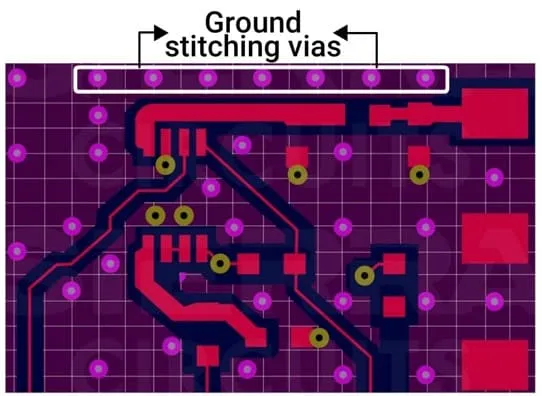
Be mindful of breaks in the ground plane. Avoid splitting it with large traces or components, as this can create isolated islands, disrupting the return path and potentially increasing noise. If splits are unavoidable, use stitching vias or small bridges to maintain continuity.
For noise sensitive circuits, place components strategically. Keep high speed signals or noisy components away from sensitive analog parts, using the ground plane as a barrier. Following these steps will help reduce noise and signaling problems in your initial designs.
Understanding the Etching Process for Ground Planes
The etching process is a critical step in quick turn PCB fabrication, especially when creating a ground plane. Etching removes unwanted copper from the board to form your desired traces and planes. For hobbyists making boards at home, understanding this process ensures the ground plane is formed correctly.
Start with a copper clad board, which is a substrate coated with a thin layer of copper on one or both sides. After designing your PCB layout, transfer the pattern onto the board using a method like toner transfer or photoresist. The ground plane area should be marked as a protected region that remains unetched.
During etching, submerge the board in a chemical solution, typically ferric chloride, which dissolves the exposed copper while leaving the protected areas intact. Ensure the solution is handled safely with proper protective gear and ventilation. The large copper area of the ground plane will remain after etching, providing the continuous conductive surface needed.
Post etching, inspect the board for defects. Ensure the ground plane is uniform without unintended breaks or thin spots, as these can affect performance. This process, while simple, requires attention to detail to maintain the integrity of your design.

Best Practices for Ground Plane Design
To maximize the benefits of a ground plane in your first circuit, follow these best practices. Always aim for a continuous, unbroken plane. If components or traces must cross it, use vias to connect separated sections, maintaining a unified return path. This helps to reduce noise and signaling problems effectively.
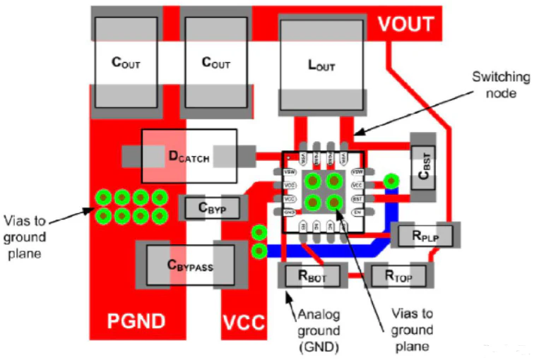
Place decoupling capacitors close to power pins of integrated circuits, connecting them directly to the ground plane. This minimizes voltage fluctuations and noise in the circuit. Also, avoid routing high speed signals over splits in the ground plane, as this can introduce interference.
Consider the board's thermal needs. If your circuit includes heat generating components, ensure the ground plane extends beneath them to dissipate heat efficiently. For multilayer designs, dedicate an entire layer to ground if possible, as this provides the best shielding and return path.
Finally, adhere to basic design rules for trace spacing and width as outlined in industry standards like IPC 2221B. These guidelines ensure your board remains manufacturable and reliable, even as a beginner project.
Common Mistakes to Avoid
Beginners often make simple errors when implementing a ground plane. One common mistake is creating splits or gaps in the plane without proper connections. This disrupts current flow, leading to noise issues. Always check for continuity across the entire plane.
Another error is neglecting to connect all ground pins to the plane. Missing connections can cause components to operate unpredictably. Double check each component's ground connection in your design before finalizing the layout.
Overloading the ground plane with unnecessary vias or cuts is also problematic. While vias are useful, excessive use can weaken the plane's effectiveness. Use them only where needed to maintain a clean, effective design.
Lastly, during the etching process, inadequate protection of the copper area can lead to uneven planes. Ensure your transfer method or resist application is precise to avoid etching away parts of the ground plane unintentionally.
Conclusion
Incorporating a ground plane into your first circuit as an electronic hobbyist is a powerful step toward creating reliable and efficient PCB designs. It offers practical benefits like helping to simplify routing, working to reduce noise and signaling problems, and aiding to dissipate heat effectively. By understanding its technical principles and following best practices, you can avoid common pitfalls and ensure your projects perform as intended. The etching process, while requiring care, is manageable with basic tools and attention to detail. As you gain experience, the ground plane will become a cornerstone of your designs, paving the way for more complex and successful circuits.
FAQs
Q1: How does a ground plane help to simplify routing for beginners?
A1: A ground plane eliminates the need for individual ground traces to each component. By connecting ground pins directly to the plane, hobbyists can reduce clutter in their PCB layout. This makes the design process faster and easier to manage, especially for first time projects with limited experience in trace planning.
Q2: Can a ground plane really reduce noise and signaling problems in simple circuits?
A2: Yes, a ground plane stabilizes the reference voltage and provides a low impedance return path for currents. This minimizes electromagnetic interference, reducing noise and signaling problems even in basic circuits. For hobbyists, it ensures more consistent performance in projects like LED drivers or simple microcontrollers.
Q3: How does a ground plane dissipate heat in a PCB design?
A3: A ground plane's large copper area acts as a thermal spreader, distributing heat generated by components across the board. This prevents hot spots and protects parts from overheating. For beginners, it adds a layer of safety in designs with power hungry components, enhancing circuit longevity.
Q4: What should I watch for during the etching process of a ground plane?
A4: During the etching process, ensure the ground plane area is properly protected by resist or toner to avoid unintended copper removal. Use safe handling practices with chemicals like ferric chloride. Inspect the board afterward for uniform copper coverage to maintain the plane's effectiveness in your circuit.
References
IPC-2221B — Generic Standard on Printed Board Design. IPC, 2012.
IPC-A-600K — Acceptability of Printed Boards. IPC, 2020.