Introduction
Satellite communication systems demand exceptional precision in design and performance due to their operation in harsh environments and reliance on high-frequency signals. High-frequency PCB layout techniques are critical for ensuring signal integrity, minimizing interference, and optimizing power efficiency in these systems. This article explores the specialized approaches required for RF PCB design and microwave PCB layout, focusing on satellite applications. Key areas such as impedance matching and microstrip antenna PCB integration will be discussed to provide actionable insights for engineers. The goal is to address the unique challenges of satellite PCB layout, where reliability and performance directly impact mission success. By understanding these principles, designers can create robust solutions for modern communication needs.
What Is High-Frequency PCB Layout and Why It Matters
High-frequency PCB layout refers to the design and arrangement of printed circuit boards operating at frequencies typically above 100 MHz, often extending into the gigahertz range for satellite communication systems. These layouts are essential for RF PCB design and microwave PCB layout, as they handle signals where even minor discrepancies can lead to significant performance degradation. In satellite systems, high-frequency PCBs are the backbone of transceivers, antennas, and signal processing units.
The importance of precise satellite PCB layout lies in maintaining signal integrity and minimizing losses. At high frequencies, issues like crosstalk, electromagnetic interference, and impedance mismatches become prominent. A poorly designed layout can result in signal distortion or complete communication failure, which is catastrophic for satellite missions. Therefore, engineers must prioritize specialized techniques to ensure reliability and efficiency in these critical applications.
Technical Principles of High-Frequency PCB Layout for Satellite Systems
Understanding Signal Behavior at High Frequencies
At high frequencies, signals behave differently compared to low-frequency circuits. They exhibit wave-like characteristics, making transmission line effects significant. In RF PCB design, traces act as transmission lines where signal propagation speed and reflections must be carefully managed. Satellite communication systems often operate in the microwave frequency range, requiring meticulous attention to trace geometry and material properties to prevent signal loss.
Electromagnetic interference is another concern. High-frequency signals can couple between adjacent traces or components, leading to noise. This is particularly problematic in satellite PCB layout, where space constraints demand dense component placement. Engineers must account for these interactions during the design phase to avoid performance issues.
Importance of Impedance Matching
Impedance matching is a cornerstone of high-frequency design, ensuring maximum power transfer between components. In microwave PCB layout, mismatched impedances cause signal reflections, leading to loss of data or reduced system efficiency. For satellite systems, where power is often limited, achieving proper impedance matching is non-negotiable.
Controlled impedance traces are used to maintain consistent impedance values across the PCB. This involves precise calculation of trace width, thickness, and spacing relative to the dielectric material. Standards such as IPC-2141A provide guidelines for designing controlled impedance circuits, ensuring compliance with industry expectations. Without proper matching, satellite communication systems risk signal degradation over long distances.
Role of Microstrip Antenna PCB Integration
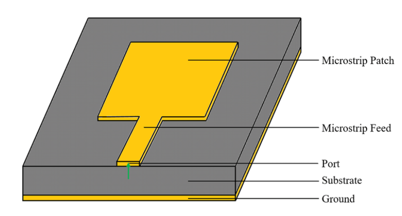
Microstrip antennas are widely used in satellite systems due to their compact size and lightweight construction. A microstrip antenna PCB consists of a radiating patch on a dielectric substrate with a ground plane beneath. This design is ideal for high-frequency applications but requires careful integration into the overall layout.
The placement of the microstrip antenna affects signal radiation patterns and impedance characteristics. Engineers must ensure that feed lines connecting to the antenna maintain consistent impedance to avoid reflections. Additionally, surrounding components should be positioned to minimize interference with the antenna’s operation. Proper design of microstrip antenna PCB layouts enhances the performance of satellite communication systems.
Related Reading: Microvia PCB for RF Applications: Design Considerations for High Frequency Performance
Practical Solutions for High-Frequency PCB Layout in Satellite Systems
Material Selection for High-Frequency Performance
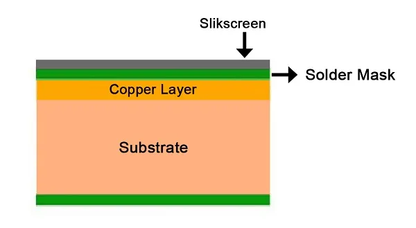
Choosing the right substrate material is vital for RF PCB design and microwave PCB layout. High-frequency signals require materials with low dielectric loss and stable electrical properties across temperature variations. Common materials used in satellite PCB layout must meet stringent requirements for thermal stability and mechanical strength due to the extreme conditions of space.
Dielectric constant and loss tangent are key parameters to consider. Materials with a low loss tangent minimize signal attenuation, which is crucial for long-distance communication in satellite systems. Engineers should refer to standards like IPC-4101E for specifications on laminate materials suitable for high-frequency applications. Selecting the appropriate material sets the foundation for a reliable design.
Trace Routing and Geometry Optimization
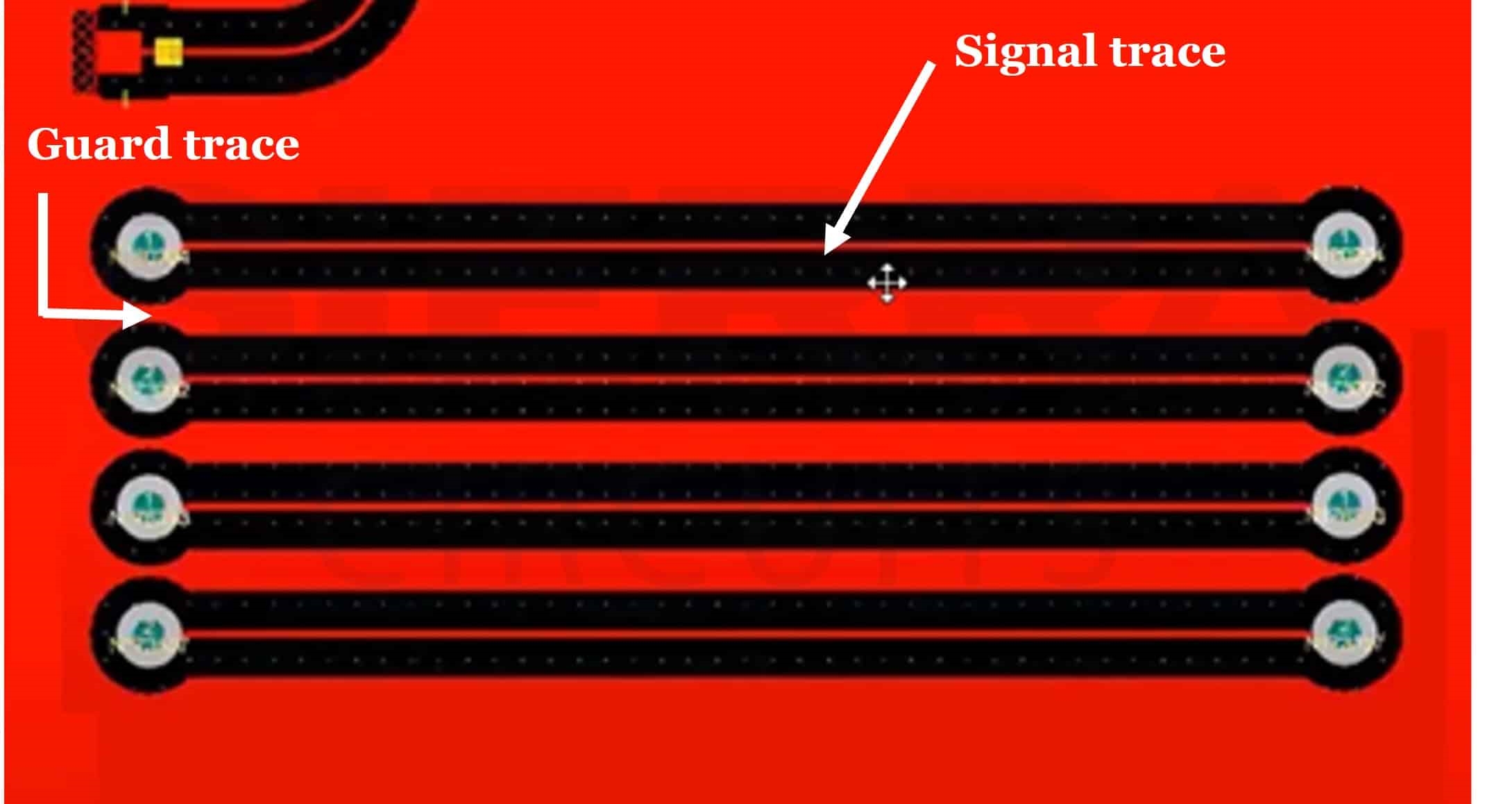
Trace routing in high-frequency PCB demands precision to avoid signal degradation. Sharp bends in traces can cause signal reflections, so engineers should use smooth curves or mitered corners. In microwave PCB layout, maintaining uniform trace width ensures consistent impedance along the signal path.
Separation between traces is equally important to reduce crosstalk. Guidelines from standards such as IPC-2221B recommend minimum spacing based on signal frequency and voltage levels. For satellite PCB layout, where board space is limited, balancing density with signal isolation is a critical challenge. Proper routing techniques preserve signal integrity under these constraints.
Ground Plane Design for Signal Integrity
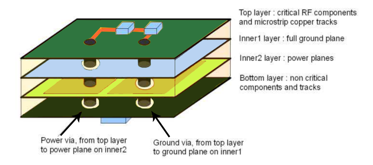
A solid ground plane is essential for high-frequency PCB layouts. It provides a low-impedance return path for signals and helps shield against electromagnetic interference. In RF PCB design, a continuous ground plane beneath signal traces minimizes noise and stabilizes impedance.
For satellite systems, multilayer PCBs often incorporate dedicated ground layers. Vias connecting to the ground plane should be strategically placed to avoid creating unintended signal paths. Adhering to best practices outlined in IPC-2222A for sectional design standards ensures effective grounding. A well-designed ground plane is fundamental to achieving reliable performance in microwave PCB layout.
Component Placement Strategies
Component placement in high-frequency designs must prioritize signal flow and minimize interference. Sensitive components, such as amplifiers and oscillators, should be isolated from noisy elements like power supplies. In satellite PCB layout, thermal management is also a concern, as components must withstand extreme temperature fluctuations.
Placing decoupling capacitors close to power pins reduces noise in the power distribution network. For microstrip antenna PCB designs, the antenna should be positioned away from other high-frequency components to avoid coupling effects. Following layout guidelines from standards like IPC-7351B for component footprints aids in achieving optimal placement.
Related Reading: PCB Component Placement for EMC Compliance: Reducing Interference
Simulation and Testing for Validation
Before fabrication, simulation tools are indispensable for validating high-frequency PCB layouts. These tools analyze signal integrity, impedance matching, and electromagnetic compatibility. For satellite communication systems, simulations must account for environmental factors like vacuum and radiation exposure.
Post-fabrication testing is equally important. Standards such as IPC-6012E outline performance specifications for rigid printed boards, including tests for signal integrity and thermal reliability. Conducting thorough testing ensures that the satellite PCB layout meets mission-critical requirements. Validation at every stage mitigates risks in high-stakes applications.
Troubleshooting Common Issues in High-Frequency Satellite PCB Layout
High-frequency designs often encounter specific challenges that require targeted solutions. One common issue is signal reflection due to impedance mismatches. Engineers can address this by recalculating trace dimensions and verifying dielectric properties against standards like IPC-2141A. Adjusting layouts to achieve proper impedance matching resolves reflection problems.
Another frequent concern is electromagnetic interference affecting signal quality. Adding shielding or revising ground plane configurations can mitigate this. For microstrip antenna PCB designs, interference from nearby components may disrupt radiation patterns. Repositioning elements or using isolation techniques helps maintain performance. Troubleshooting requires a systematic approach to identify and correct layout flaws.
Conclusion
High-frequency PCB layout techniques are indispensable for the success of satellite communication systems. By focusing on critical aspects like impedance matching, material selection, and microstrip antenna PCB integration, engineers can design robust solutions for challenging environments. Adhering to established standards ensures consistency and reliability in RF PCB design and microwave PCB layout. As satellite technology advances, mastering these techniques will remain essential for maintaining seamless communication. A methodical approach to satellite PCB layout empowers designers to meet the stringent demands of modern missions.
FAQs
Q1: How does impedance matching impact satellite PCB layout performance?
A1: Impedance matching is crucial in satellite PCB layout as it ensures maximum power transfer and minimizes signal reflections. Mismatched impedances lead to data loss and reduced efficiency, which is critical in power-constrained satellite systems. Following industry guidelines for controlled impedance helps maintain signal integrity across high-frequency traces.
Q2: What materials are best for high-frequency RF PCB design in satellite systems?
A2: For RF PCB design in satellite systems, materials with low dielectric loss and thermal stability are preferred. These properties reduce signal attenuation and ensure reliability in space conditions. Standards like IPC-4101E provide specifications for suitable laminates, guiding engineers in selecting materials for optimal performance.
Q3: Why is microstrip antenna PCB integration important for satellite communication?
A3: Microstrip antenna PCB integration is vital for satellite communication due to its compact and lightweight design. Proper placement and impedance control of the antenna ensure efficient signal radiation and reception. This integration directly affects communication reliability, making it a key focus in high-frequency layouts.
Q4: What are common challenges in microwave PCB layout for satellite applications?
A4: Microwave PCB layout for satellite applications faces challenges like signal loss, interference, and thermal stress. High frequencies amplify issues such as crosstalk and impedance mismatches. Addressing these requires precise trace routing, effective grounding, and adherence to standards like IPC-2221B for reliable operation in harsh environments.
References
IPC-2141A — Design Guide for High-Speed Controlled Impedance Circuit Boards. IPC, 2004.
IPC-4101E — Specification for Base Materials for Rigid and Multilayer Printed Boards. IPC, 2017.
IPC-2221B — Generic Standard on Printed Board Design. IPC, 2012.
IPC-2222A — Sectional Design Standard for Rigid Organic Printed Boards. IPC, 2010.
IPC-7351B — Generic Requirements for Surface Mount Design and Land Pattern Standard. IPC, 2010.
IPC-6012E — Qualification and Performance Specification for Rigid Printed Boards. IPC, 2020.