Introduction
High-speed PCB stackup design forms the foundation of reliable signal integrity in modern electronics. As data rates climb into gigabits per second, engineers face challenges from impedance mismatches and signal loss that degrade performance. A well-planned stackup ensures controlled impedance and minimal attenuation across transmission lines. This article explores the principles behind high-speed PCB stackup, focusing on impedance control and signal loss mitigation. Electrical engineers will find structured insights into microstrip and stripline configurations, along with trace width calculation strategies. Mastering these elements leads to robust designs that meet stringent performance demands.
What Is High-Speed PCB Stackup and Why It Matters
A high-speed PCB stackup refers to the arrangement of conductive layers, dielectrics, and planes in a multilayer board optimized for signals exceeding 1 GHz. It directly influences characteristic impedance, crosstalk, and propagation delay. Poor stackup choices amplify reflections and attenuation, causing bit errors in high-speed interfaces. Impedance control becomes critical to match source and load impedances, typically targeting 50 ohms or 100 ohms differential. Signal loss, meanwhile, accumulates from material properties and geometry, demanding precise layer sequencing. In industries like telecommunications and computing, effective stackup design ensures compliance with performance specs and reduces redesign iterations.
Engineers prioritize stackup early in the design cycle because it dictates routing feasibility and material selection. Symmetric builds prevent warpage, while plane proximity minimizes inductance. These factors matter for maintaining eye diagram integrity and passing compliance tests. High-speed PCB stackup thus bridges theory and fabrication, enabling signals to travel with fidelity over long traces.
Fundamental Principles of Impedance Control
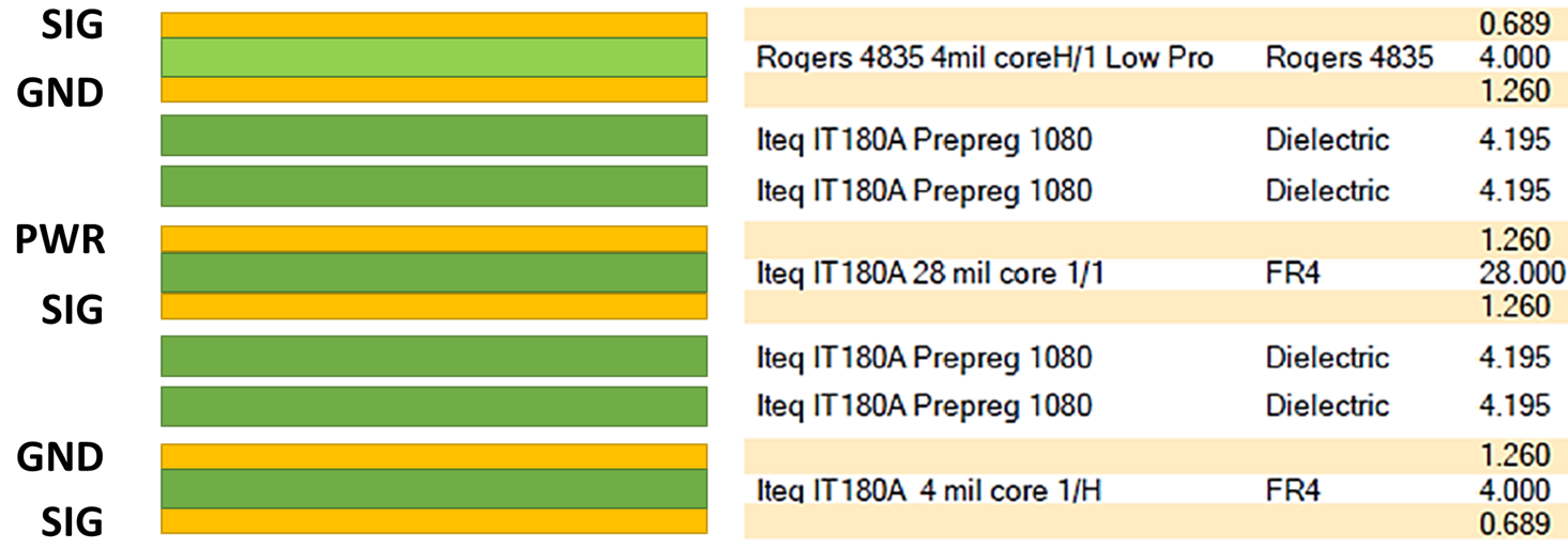
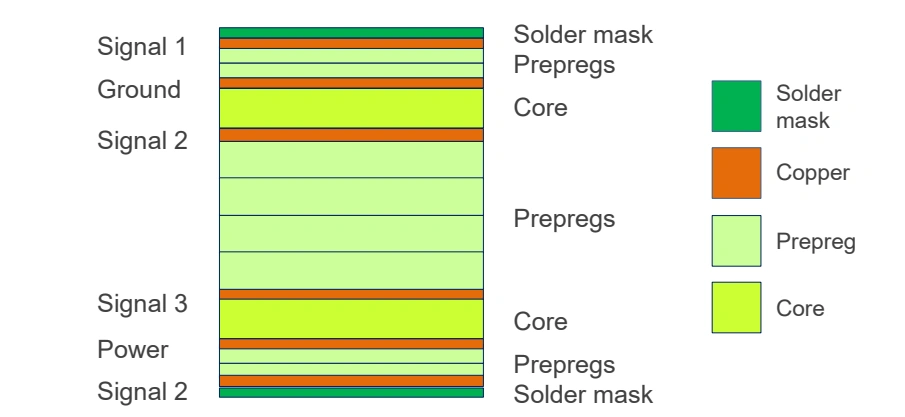
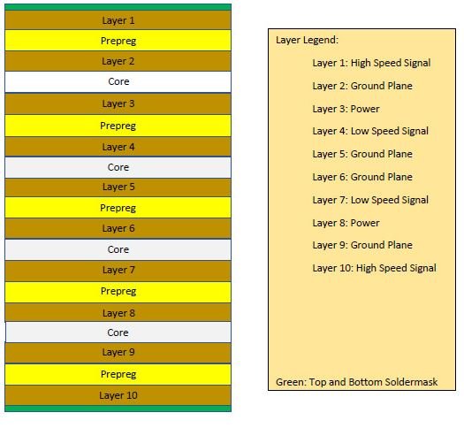
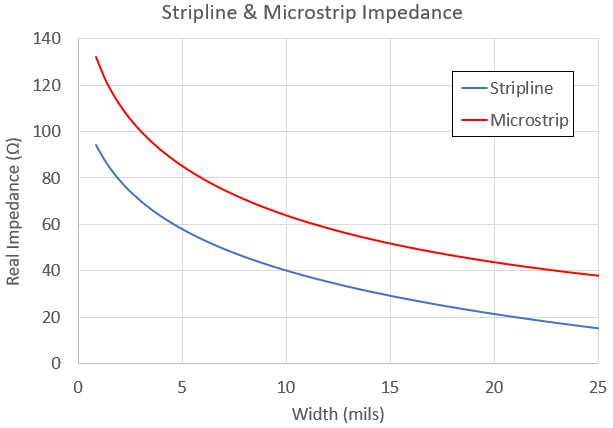
Impedance control in high-speed PCB stackup revolves around maintaining consistent characteristic impedance along transmission lines. Characteristic impedance depends on trace geometry, dielectric constant, and reference plane distance. Microstrip lines, positioned on outer layers with air and dielectric above, offer easier fabrication but higher radiation losses. Striplines, embedded between ground planes, provide better shielding and lower crosstalk at the cost of tighter tolerances. Engineers calculate impedance using formulas that balance width, thickness, and height to ground.
Trace width calculation starts with target impedance and material properties. Wider traces lower impedance in microstrips due to increased capacitance, while narrower ones suit striplines for the same goal. Dielectric height critically affects field distribution; thinner dielectrics raise impedance unless compensated by width. Field solvers verify these interactions, but initial estimates guide stackup planning. Consistent prepreg and core thicknesses ensure uniformity across the board.
Reference planes act as return paths, forming transmission line structures essential for impedance control. Voids or splits in planes disrupt this, causing impedance discontinuities. Plane stitching vias mitigate these effects by providing low-inductance paths. In high-speed PCB stackup, alternating signal and plane layers optimizes this balance.
Suggested Reading: Optimizing PCB Stackup for Differential Impedance Control: A Step by Step Guide
Mechanisms of Signal Loss in High-Speed PCBs
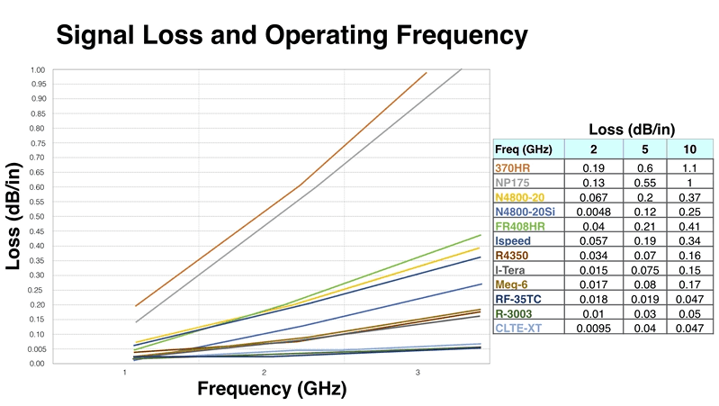
Signal loss in high-speed designs arises from conductor, dielectric, and radiative mechanisms, each amplified by frequency. Conductor loss stems from skin effect, where current flows near the surface, increasing effective resistance. At multi-GHz frequencies, this loss scales with square root of frequency, narrowing the usable bandwidth. Dielectric loss, quantified by the loss tangent, dissipates energy as heat in the insulator. Materials with low dissipation factor preserve signal amplitude over distance.
Geometry exacerbates these losses; longer traces accumulate more attenuation. Microstrips suffer additional radiation loss due to exposed fields, unlike fully enclosed striplines. Vias introduce insertion loss through transitions between layers. Engineers model total loss as dB per inch, factoring frequency dependence. Minimizing trace length and bends reduces overall degradation.
Crosstalk and reflections compound effective signal loss by distorting waveforms. Aggressive stackups with tight spacing heighten coupling between adjacent traces. Proper clearance and guard traces counteract this. Understanding these mechanisms guides stackup choices for low-loss performance.
Best Practices for High-Speed PCB Stackup Design
Start high-speed PCB stackup with symmetric layer pairing to avoid bow and twist. Core and prepreg selection prioritizes low-loss dielectrics with stable constants. Place high-speed signals on inner layers as striplines for confinement, reserving microstrips for lower-speed nets. Reference planes should sandwich signal layers with uniform dielectric thickness. This configuration supports precise impedance control and curbs signal loss.
Trace width calculation requires iterative adjustment based on stackup parameters. Target uniform heights to ground across pairs for differential signaling. Incorporate plane capacitance for power integrity, reducing noise coupling. Vias demand back-drilling or blind configurations to minimize stubs that reflect signals. Fabricators appreciate 1:1 core-to-prepreg ratios for lamination stability.
IPC-2221 guidelines emphasize controlled impedance through geometry and materials. Layer count influences thermal management; even-odd builds suit high-speed needs. Simulate stackup early to predict losses and adjust widths. Ground pour fill on outer layers aids shielding without excess loss.
For dense designs, hybrid stackups blend microstrip and stripline zones. Power planes offset from signals prevent resonance. These practices, aligned with IPC-6012 specifications for performance, yield manufacturable boards. Testing verifies impedance with time-domain reflectometry.
Troubleshooting Common Stackup Challenges
Engineers often encounter impedance variations from fabrication tolerances. Measure coplanarity post-lamination to catch dielectric inconsistencies. Signal loss spikes signal poor material matching between layers. Cross-section analysis reveals plating voids contributing to conductor loss. Adjust trace widths conservatively to account for etch shrinkage.
Crosstalk troubleshooting involves lengthening return paths or adding shielding. J-STD-001 standards guide assembly to preserve stackup integrity. Simulate before committing to prototypes. These steps resolve most issues without full respins.
Suggested Reading: Troubleshooting PCB Stackup Issues: Identifying and Resolving Signal Integrity Problems
Conclusion
High-speed PCB stackup design demands mastery of impedance control and signal loss mitigation for signal integrity. Microstrip and stripline choices, paired with precise trace width calculation, form the core strategy. Best practices like symmetric builds and reference plane proximity ensure low attenuation and minimal reflections. Adhering to industry standards elevates design reliability. Electrical engineers applying these principles achieve first-pass success in demanding applications.
FAQs
Q1: What factors most influence impedance control in high-speed PCB stackup?
A1: Impedance control hinges on trace width, dielectric thickness, and reference plane proximity. Microstrip lines demand wider traces for lower impedance compared to striplines due to partial air dielectric. Material constants and copper weight also play roles. Engineers iterate calculations to hit targets like 50 ohms single-ended. Consistent stackup geometry across the board prevents variations.
Q2: How does signal loss differ between microstrip and stripline in high-speed designs?
A2: Microstrip incurs higher signal loss from radiation and surface skin effect exposure. Stripline confines fields between planes, reducing dielectric and radiative losses. Conductor loss remains similar but benefits from smoother embedding. For long traces, stripline preserves integrity better. Stackup choice balances this with routing needs.
Q3: Why is trace width calculation critical for high-speed PCB stackup?
A3: Trace width calculation sets characteristic impedance and controls loss tangent impact. Narrow traces raise resistance via skin effect, while wide ones increase capacitance. It ensures matching for minimal reflections. Variations cause eye closure in high-speed signals. Precise computation supports overall stackup optimization.
Q4: What role do reference planes play in minimizing signal loss?
A4: Reference planes provide return paths, lowering inductance and containing fields. They reduce crosstalk and radiation in stripline setups. Proximity to signals cuts propagation delay. Planes also distribute heat evenly. Proper placement is key to low signal loss in high-speed PCB stackup.
References
IPC-2221B — Generic Standard on Printed Board Design. IPC, 2009
IPC-6012E — Qualification and Performance Specification for Rigid Printed Boards. IPC, 2015
J-STD-001H — Requirements for Soldered Electrical and Electronic Assemblies. IPC, 2018