Why is Trace Width an Important Factor in PCB Impedance?
For electrical engineers involved in printed circuit board (PCB) design, understanding how trace width influences impedance is fundamental. Simply put, the characteristic impedance of a PCB trace is directly impacted by its width: broader traces lead to lower impedance, while narrower ones result in higher impedance. This interaction is crucial for maintaining signal integrity and optimal performance, especially in high-speed circuit applications where precise impedance matching is paramount.
PCB design goes beyond merely placing components and routing connections; it's about ensuring signals transmit accurately without degradation or loss. Impedance, which quantifies a circuit's opposition to alternating current, plays a significant role in preventing issues like signal reflections, crosstalk, and data errors that are common in high-frequency or high-speed digital systems if not properly controlled.
The Critical Role of Controlled Impedance
In high-speed contexts, maintaining a consistent characteristic impedance—often 50 ohms for RF circuits or 90-100 ohms for differential pairs like those found in USB—is vital for avoiding signal reflections. A discrepancy between the trace's impedance and that of the source or load can cause portions of the signal to bounce back, introducing noise and potential errors. Trace width stands out as one of the primary elements dictating this impedance.
Whether you're working on designs for USB, HDMI, or radio frequency (RF) applications, a solid grasp of how PCB trace width and impedance are connected is indispensable. This relationship ensures that signals flow efficiently, preventing distortions and maintaining the integrity of transmitted data.
What Does "Impedance" Mean in PCB Layout?
Before delving into the specifics of trace width, it helps to clarify the concept of impedance within the realm of PCBs. Impedance, commonly symbolized as Z₀, represents the total resistance a circuit offers to alternating current. It's a composite measure, incorporating both the electrical resistance inherent in the trace material and the reactance arising from its inductance and capacitance. In PCB engineering, discussions usually center on "characteristic impedance," which is the inherent impedance of a transmission line, such as a trace, envisioned as infinitely long.
Ensuring consistent characteristic impedance for high-speed signals is paramount to prevent unwanted signal reflections. For instance, RF designs often target 50 ohms, while differential pairs, as seen in USB, might require 90-100 ohms. If a trace's impedance doesn't align with its source or load, a portion of the signal can reflect backward, leading to noise and data inaccuracies. Several elements shape this impedance, including the trace's width and thickness, the dielectric material used, and its proximity to ground planes.
How Does PCB Trace Width Directly Influence Impedance?
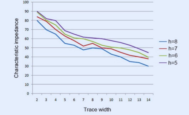
The relationship between trace width and impedance is straightforward yet profoundly impactful: as a trace becomes wider, its impedance decreases, and conversely, a narrower trace results in higher impedance. This behavior can be attributed to two fundamental electrical properties: capacitance and inductance.
Capacitance and Inductance Effects
● Capacitance: A wider trace presents a larger surface area to the adjacent ground plane. This increased surface area enhances the capacitance between the trace and the ground. Since higher capacitance directly correlates with lower impedance, a wider trace effectively reduces the overall impedance of the signal path.
● Inductance: Conversely, a narrower trace concentrates the magnetic field lines more densely. This concentration leads to higher inductance. As increased inductance contributes to higher impedance, a narrower trace will, therefore, raise the signal's impedance.
Consider a practical example: a microstrip configuration, where a trace resides on the top layer above a ground plane. A 10-mil (0.254 mm) wide trace on a standard FR-4 substrate (dielectric constant, Dk, of approximately 4.5, and a height of 1.6 mm) might yield a characteristic impedance of 50 ohms. If this trace is widened to 20 mils (0.508 mm), the impedance could drop to around 35 ohms due to the increased capacitance. Conversely, reducing the width to 5 mils (0.127 mm) might elevate the impedance to 75 ohms or more. This clear correlation makes adjusting trace width a primary strategy for achieving target impedance values in PCB layout, particularly in RF designs requiring 50-ohm impedance or high-speed digital circuits needing 90-100 ohms for differential pairs.
What Other Factors Affect Trace Impedance?
While trace width is a significant determinant, several other elements also play a crucial role in shaping a PCB trace's impedance. A holistic understanding of these factors is essential for precise impedance control and optimal design performance.
● Trace Thickness: The thickness of the copper trace itself contributes to its impedance, albeit to a lesser extent than its width. Thicker traces generally reduce resistance, which can have a minor effect on impedance. Standard copper thickness is often 1 oz/ft² (approximately 35 μm), but thicker options like 2 oz/ft² (70 μm) are used for applications requiring higher current capacity.
● Dielectric Constant (Dk): The dielectric material situated between the trace and its ground plane significantly influences capacitance. Materials such as FR-4 typically have a Dk of around 4.5. However, materials with lower Dk values, like those found in Rogers substrates, are often chosen for high-frequency designs to help maintain signal integrity by reducing capacitance and thus managing impedance more effectively.
● Height Above Ground Plane: The physical distance separating the trace from its ground plane directly impacts capacitance. A smaller separation distance increases capacitance, leading to a reduction in impedance. Conversely, a greater height above the ground plane will decrease capacitance and increase impedance.
● Trace Length and Routing: Although trace length does not inherently alter the characteristic impedance of a transmission line, it profoundly affects signal delay and overall signal loss, which are critical components of a circuit's performance. The way a trace is routed, including bends and turns, can also introduce minor discontinuities that affect impedance.
An awareness of how these various factors interrelate with trace width enables engineers to meticulously fine-tune their designs, achieving the most favorable performance characteristics for their specific applications.
Suggested Reading: Understanding Trace Width Tolerances in PCB Manufacturing for Reliable Designs
How Do You Calculate Trace Width for Specific Impedance?
Determining the precise trace width needed for a target impedance is a critical step in PCB design. While manual calculations can involve intricate equations, understanding the fundamental process, especially for a common microstrip trace, is beneficial.
Step-by-Step Calculation for Microstrip Traces
1. Define Your Target Impedance (Z₀): Begin by establishing the desired impedance value for your trace. For example, RF applications commonly require 50 ohms, while USB differential pairs often target 90 ohms.
2. Gather Essential PCB Parameters: You'll need specific information about your PCB stack-up:
a. Dielectric Constant (Dk): The relative permittivity of your substrate material (e.g., approximately 4.5 for FR-4).
b. Dielectric Height (H): The distance between the trace and its ground plane (e.g., 1.6 mm for a standard two-layer PCB). Ensure consistent units with trace width and thickness.
c. Copper Thickness (T): The thickness of the copper trace, typically 35 μm for 1 oz copper.
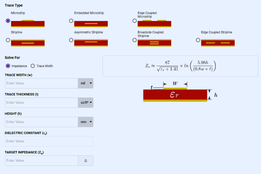
3. Apply the Microstrip Impedance Formula: The characteristic impedance (Z₀) of a microstrip can be approximated using the following formula:
Z₀ = (87 / √(Dk + 1.41)) * ln(5.98H / (0.8W + T))
Where:
a. Z₀ represents the characteristic impedance (in ohms).
b. Dk is the dielectric constant of the substrate.
c. H is the height of the dielectric layer.
d. W is the trace width (the value you are solving for).
e. T is the trace thickness.
Solving this equation directly for W (trace width) by hand can be challenging. For example, to achieve a 50-ohm impedance on an FR-4 board (Dk=4.5, H=1.6 mm, T=35 μm), the approximate trace width (W) might be around 2.9 mm. However, this value will vary based on the exact material properties and stack-up configuration.
4. Validate with Simulation Software or Online Tools: Due to the approximations inherent in manual calculations and the complexity of the formula, it is always advisable to verify your results using specialized PCB design software (such as Altium Designer or KiCad) or reliable online PCB trace impedance calculators. These tools incorporate more precise models and account for various real-world parameters, providing more accurate and dependable outcomes.
How Can PCB Trace Impedance Calculators Help?
For many engineers, manually calculating trace width is often inefficient and prone to errors. Modern software tools, particularly PCB trace impedance calculators, offer a streamlined and accurate alternative. These calculators are widely available online or as integrated features within professional PCB design software.
Steps for Using an Impedance Calculator
1. Input Key Parameters: Begin by entering the necessary values into the calculator. This typically includes your target impedance (e.g., 50 ohms), the dielectric constant (Dk) of your substrate (e.g., 4.5), the dielectric height (H) between the trace and its ground plane (e.g., 1.6 mm), and the copper thickness (T) (e.g., 35 μm).
2. Select Trace Configuration: Specify the type of transmission line you are designing—most commonly, a microstrip (a trace situated over a ground plane) or a stripline (a trace embedded between two ground planes).
3. Retrieve Results: The calculator will promptly provide the required trace width (W) that corresponds to your specified parameters. For instance, if you input parameters for a 50-ohm impedance on a 1.6 mm FR-4 board, the calculator might suggest a width of approximately 2.8 to 3.0 mm.
Numerous free tools are available from reputable providers like AdvancedPCB and MCLPCB, among others frequently discussed in engineering communities. These calculators often allow for real-time adjustments of parameters, enabling engineers to quickly observe how changes in trace width or material properties impact impedance, making them invaluable for rapid design iterations and optimization.
Practical Strategies for Managing Impedance Through Trace Width
Controlling impedance effectively using trace width is a vital skill for electrical engineers. Here are several actionable strategies to help ensure signal integrity in your PCB designs:
● Adhere to Industry Standards: Always begin your design process by referencing established industry impedance standards (e.g., 50 ohms for RF circuits or 100 ohms for differential pairs). Use these as a baseline, then adjust your trace widths accordingly to achieve precise matching.
● Collaborate on Stack-Up Data: Engage directly with your online PCB manufacturer to confirm the exact dielectric constants and layer heights of their materials. Even minor variations in substrate properties can lead to impedance shifts of 5-10%, impacting performance.
● Prioritize Smooth Routing: When routing traces, opt for 45-degree angles or smooth curves instead of abrupt 90-degree bends. This practice minimizes impedance discontinuities that can cause signal reflections.
● Thorough Simulation and Iteration: After determining initial trace widths, it is crucial to simulate your design using specialized tools such as HyperLynx or Ansys. This verification step helps confirm expected performance before committing to fabrication, potentially preventing costly redesigns.
● Account for Manufacturing Variances: Recognize that trace width can fluctuate by as much as ±10% during manufacturing. Incorporate a small margin into your design or, if impedance is highly critical, specify tighter manufacturing tolerances to your fabricator.
For example, when designing a recent 5G RF board that required 50-ohm traces for antenna connections, I used an online PCB trace impedance calculator to determine a preliminary width of 2.85 mm for a two-layer FR-4 PCB board. Following simulations, I slightly adjusted the width to 2.9 mm to mitigate potential manufacturing variations. Post-fabrication testing confirmed that the impedance was within 2% of the target, well within acceptable performance limits.
Common Pitfalls to Avoid in Impedance Control
Even seasoned engineers can encounter challenges when managing trace width and impedance. Being aware of frequent errors can help prevent significant design issues:
● Ignoring Dielectric Material Variations: Assuming a fixed dielectric constant (Dk), such as 4.5 for FR-4, without validating the actual value with your PCB manufacturer can lead to significant impedance mismatches. Dk values can realistically range from 4.2 to 4.8, and these small differences accumulate.
● Overlooking Crosstalk from Adjacent Traces: Traces routed too closely together can induce crosstalk, which effectively alters their impedance. To maintain signal isolation and consistent impedance, ensure adequate spacing—often recommended as three times the trace width—between critical traces.
● Neglecting Ground Plane Integrity: A discontinuous or poorly designed ground plane beneath critical traces can severely disrupt impedance control. It is essential to ensure a robust and continuous ground plane to provide a stable reference for signal propagation.
Mastering Trace Width for Optimal PCB Performance
A deep understanding of how PCB trace width impacts impedance is an indispensable skill for any electrical engineer engaged in high-speed or high-frequency circuit design. By thoroughly grasping the intricate relationship between PCB trace width and impedance, and by proficiently utilizing methods to calculate the appropriate trace width for desired impedance, supported by advanced tools like PCB trace impedance calculators, you can effectively guarantee signal integrity and circumvent expensive design revisions.
It is crucial to remember the core principle: wider traces inherently lead to lower impedance, while narrower traces result in higher impedance. Always rely on calculators or sophisticated design software to precisely determine the required width for your target impedance, and consistently cross-reference these calculations with simulations and detailed manufacturer data. Adopting these disciplined practices will equip you to confidently tackle the most demanding PCB design challenges, ensuring robust and reliable circuit performance.